Dr. Vadym Zayets
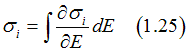
v.zayets(at)gmail.com
My Research and Inventions
click here to see all content |

Dr. Vadym Zayetsv.zayets(at)gmail.com |
|
|
more Chapters on this topic:IntroductionTransport Eqs.Spin Proximity/ Spin InjectionSpin DetectionBoltzmann Eqs.Band currentScattering currentMean-free pathCurrent near InterfaceOrdinary Hall effectAnomalous Hall effect, AMR effectSpin-Orbit interactionSpin Hall effectNon-local Spin DetectionLandau -Lifshitz equationExchange interactionsp-d exchange interactionCoercive fieldPerpendicular magnetic anisotropy (PMA)Voltage- controlled magnetism (VCMA effect)All-metal transistorSpin-orbit torque (SO torque)What is a hole?spin polarizationCharge accumulationMgO-based MTJMagneto-opticsSpin vs Orbital momentWhat is the Spin?model comparisonQuestions & AnswersEB nanotechnologyReticle 11
more Chapters on this topic:IntroductionTransport Eqs.Spin Proximity/ Spin InjectionSpin DetectionBoltzmann Eqs.Band currentScattering currentMean-free pathCurrent near InterfaceOrdinary Hall effectAnomalous Hall effect, AMR effectSpin-Orbit interactionSpin Hall effectNon-local Spin DetectionLandau -Lifshitz equationExchange interactionsp-d exchange interactionCoercive fieldPerpendicular magnetic anisotropy (PMA)Voltage- controlled magnetism (VCMA effect)All-metal transistorSpin-orbit torque (SO torque)What is a hole?spin polarizationCharge accumulationMgO-based MTJMagneto-opticsSpin vs Orbital momentWhat is the Spin?model comparisonQuestions & AnswersEB nanotechnologyReticle 11
more Chapters on this topic:IntroductionTransport Eqs.Spin Proximity/ Spin InjectionSpin DetectionBoltzmann Eqs.Band currentScattering currentMean-free pathCurrent near InterfaceOrdinary Hall effectAnomalous Hall effect, AMR effectSpin-Orbit interactionSpin Hall effectNon-local Spin DetectionLandau -Lifshitz equationExchange interactionsp-d exchange interactionCoercive fieldPerpendicular magnetic anisotropy (PMA)Voltage- controlled magnetism (VCMA effect)All-metal transistorSpin-orbit torque (SO torque)What is a hole?spin polarizationCharge accumulationMgO-based MTJMagneto-opticsSpin vs Orbital momentWhat is the Spin?model comparisonQuestions & AnswersEB nanotechnologyReticle 11
more Chapters on this topic:IntroductionScatteringsSpin-polarized/ unpolarized electronsSpin statisticselectron gas in Magnetic FieldFerromagnetic metalsSpin TorqueSpin-Torque CurrentSpin-Transfer TorqueQuantum Nature of SpinQuestions & Answers
more Chapters on this topic:IntroductionTransport Eqs.Spin Proximity/ Spin InjectionSpin DetectionBoltzmann Eqs.Band currentScattering currentMean-free pathCurrent near InterfaceOrdinary Hall effectAnomalous Hall effect, AMR effectSpin-Orbit interactionSpin Hall effectNon-local Spin DetectionLandau -Lifshitz equationExchange interactionsp-d exchange interactionCoercive fieldPerpendicular magnetic anisotropy (PMA)Voltage- controlled magnetism (VCMA effect)All-metal transistorSpin-orbit torque (SO torque)What is a hole?spin polarizationCharge accumulationMgO-based MTJMagneto-opticsSpin vs Orbital momentWhat is the Spin?model comparisonQuestions & AnswersEB nanotechnologyReticle 11
more Chapters on this topic:IntroductionTransport Eqs.Spin Proximity/ Spin InjectionSpin DetectionBoltzmann Eqs.Band currentScattering currentMean-free pathCurrent near InterfaceOrdinary Hall effectAnomalous Hall effect, AMR effectSpin-Orbit interactionSpin Hall effectNon-local Spin DetectionLandau -Lifshitz equationExchange interactionsp-d exchange interactionCoercive fieldPerpendicular magnetic anisotropy (PMA)Voltage- controlled magnetism (VCMA effect)All-metal transistorSpin-orbit torque (SO torque)What is a hole?spin polarizationCharge accumulationMgO-based MTJMagneto-opticsSpin vs Orbital momentWhat is the Spin?model comparisonQuestions & AnswersEB nanotechnologyReticle 11
|
Spin and Charge Transport near an Interface
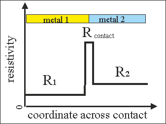
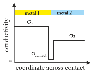
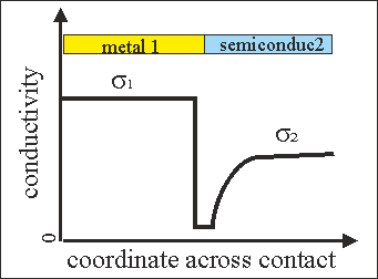
Spin and Charge TransportThe spin and charge transport in the vicinity of a contact between two metals are substantially different from the transport in the bulk of metals. In the vicinity of the contact, The probability of electron back reflection becomes larger. As a result, the number of the running-wave electrons decreases and the number of the standing-wave electrons increases compared to the bulk. In the bulk the major transport mechanism is the current of the running-wave electrons and the scattering current is often significantly smaller. In contrast, in the vicinity of an interface the current of the running-wave electrons decreases or even becomes negligible, but the scattering current increases and often became the dominant transport mechanism.The spin properties of the conduction are substantially different in the bulk and in the vicinity of an interface. If in the bulk the injection conductivity in metals and the detection conductivity in metals and semiconductors are neglegibally small. In the vicinity of the interface the injection and detection conductivities may be substantial.The conductivity at the interface becomes anisotropic. The conductivities for a current flows along and across a contact becomes different.
|
Oversimplified view of metal conduction in the vicinity of interface as assumed in the classical model |
|||||||||
|
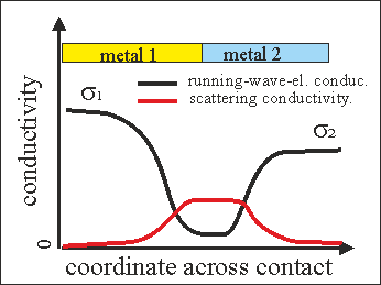
According to the presented model the conductivity through the contact does not have any step-like or delta-function-like features. The conductivity monolithically changes over a distances ~1-4 mean-free paths from the bulk conductivity of one metal to the bulk conductivity of the other metal. The running-wave conductivity decreases from the bulk conductivity of the first metal, reaches a minimum at the interface between the metals and again increases to the bulk conductivity of the second metal. The scattering conductivity changes from being negligibly small in the bulk of the metals to becoming a substantial at the interface. The scattering conductivity may even overcome the running-wave conductivity.
Conductivity near Interface. Presented Model |
||||||||||||||||
|
(1) Reduction of the number of running-wave electrons and increasing of the number of standing-wave electrons. This causes the reduction of the current of the running-wave electrons.
|
|
 |
 |
(2) The electron scattering probability in the direction toward the interface becomes smaller that the scattering probability outward the interface. This causes significant increase of the scattering current.
(1) Only the running-wave conduction. The scattering conductivity is near zero.
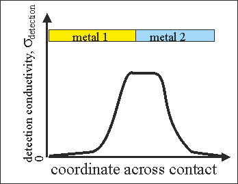
(2) The detection conductivity is near zero.
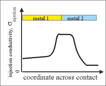
(3) The injection conductivity is near zero in a metal and it equals to the charge conductivity for a non-degenerate semiconductor.

Running-wave electron conductivity:
(1) It becomes smaller , because of a reduction of the number of the running wave electrons
(2) The detection conductivity may become substantial.
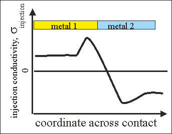
(3) The injection conductivity of a metal may become substantial.
(4) The charge conductivity may become dependent on the spin accumulation sp in a metal.
(5) The conductivity at the interface becomes anisotropic. The conductivity for a current flows along and across a contact becomes different.
The scattering conductivity
If in bulk of a metal the scattering conductivity is near zero, it becomes substantial near an interface. It is because near an interface the scattering probability of an electron to be scattered toward the interface and in opposite direction are substantially different.
There are two types of the scattering conductivity at an interface. 
(1) The first type is the scattering conductivity by the running-wave electrons. It is the conductivity of a low-resistance contact (for example, a contact between two metal)
(2) The second type is the scattering conductivity of the standing-wave electrons. It is the conductivity of a high resistance contact (for example, a tunnel junction or a contact between a metal and a semiconductor)
.
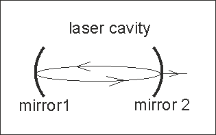
Standing-wave photon in laser cavity |
|
Photon is reflecting back and forward between two mirrors forming a standing wave. When the photon passes through the semitransparent mirror, it becomes the running-wave photon. Similarly, a standing-wave electron is reflected between two defects (note, only one defect is sufficient to make a standing wave electron) |
A contact or an interface between two metals can be considered is an obstacle for the movement of an electron. The electrons can be compared with photons of light. When light passes through the boundary between two materials, only a part of light passes through the boundary and a part of light is reflected back. Similarly for an electron, there is a finite probability that the electron is reflected from an interface and there is a finite probability the electron passes through the interface as a running-wave electron. Obviously, the electrons, which are reflected from the interface, do not transport the spin and charge through the contact. They can be considered as bounded by the interface and they become the standing-wave electrons. In the case of a contact between similar metals, the electron reflection at the contact is a small and in vicinity of contact there is a substantial number of the running-wave electrons. In contrast, the reflection is nearly full at a contact between different materials, like a metal-semiconductor or a tunnel barrier, and almost all the electrons in the vicinity of this contact are the standing-wave electrons.
 The electron mean-free path
 ![]() determines an effective length where the conductivity changes from a bulk type to an interface type.
determines an effective length where the conductivity changes from a bulk type to an interface type.
The effective length of electron interaction with interface is different for electrons of different energies and "spin" and "full" states, because of different mean-free path
|
 |
Near interface the number of the running-wave electrons increase and the number of standing-wave electrons increases. Amount of decrease of running wave electrons at a contact depends on materials of the contact. For example, in case of a contact between two similar metals the amount of the standing-wave electrons at contact is not large. In contrast, in the case of a tunnel junction all electrons at the contact are expected to be standing-wave electrons. Therefore, an interface can be characterized by a parameter, which describes a ratio of standing-wave electrons to running-wave electrons. We define this parameter as the contact reflectivity R.
The contact reflectivity R may depend
(1) Electron energy. For example in the case of a Schottky barrier, the width of the barrier is narrower for electrons of higher energy and they experience small reflectivity from the contact
(2) Temperature. The mean-free-path independent scatterings (for example, scattering on phonons) may reduce the number of the standing-wave electrons and increase the number of the running-wave electrons. It is similar to the the case of the electron transport in the bulk of metal with defects. This effect may only substantially influence the number of the running-wave electrons only in the case of a small interface reflectivity R.
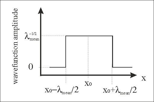 |
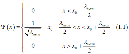
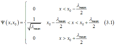
Fig.1 The electron wave function in the approximation of the square-shape wave-function. The electron moves in the x-direction. The current electron position is x0. The width of the electron. The width of the wave function equals to the electron mean-free path. Note: Within presented model the replacement of the square shape to a more-realistic Gaussian shape is straightforward. This does not change substantially the final results. |
Within the approximation of the square-shape wave-function the special distribution of the wave function of an electron moving along the x-direction at point x=x0 is approximated as
 Main idea:
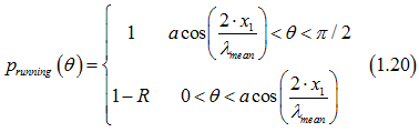
It is assumed that when the wave function of an electron (Eq. (1.1)) touches the interface, a running-wave electron becomes a standing-wave electron with the probability R, where R is defined as the reflectivity of the interface.
The number of the standing-wave electrons depends on the angle theta between the electron movement direction and the contact normal. In the case when the contact is in the yz-plane at x=0, the electron at position x=x1 touches the contact if
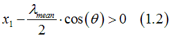
or 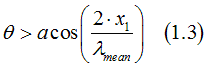
In an equilibrium the electron movement directions are distributed equally in all directions. This means that the probability that an electron moves in the direction between theta and theta+ d_theta is
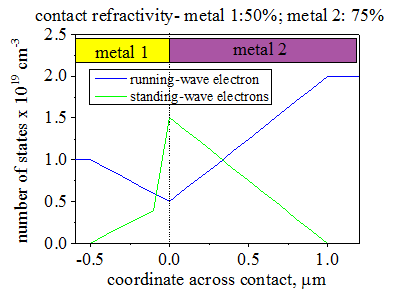
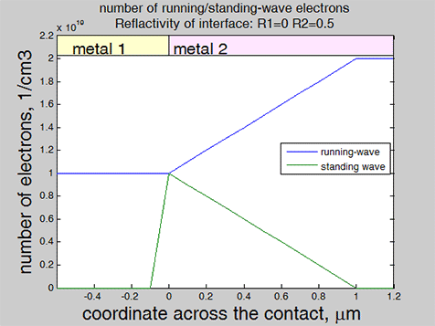
| Fig.18. Number of running-wave and standing-wave electrons in vicinity of the interface | ||
|
||
Fig.18. Number of the running-wave and standing-wave electrons in the vicinity of a contact between two metals. It is assumed that in each metal the mean-free path is the same for all electrons
Animation parameter for right figure is refractivity of the contact. Note1: In case when there is no reflectivity in metal1 is zero (R1=0), the reflectivity in metal2 is not zero R2=0.5 material parameters (click to extend)
The metal 1 (left) and metal 2 (right) are contacted at x=0. The bulk number of electrons: n1=1E19 1/cm3 (metal 1) and n2=1E19 1/cm3 (metal (2). Mean-free path: l um (metal 1) and it equals to 1 um in metal 1 and 2 um ( metal 2). |
![]()
and 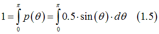
From Eqs (1.3,1.4) the condition that an electron at position x=x1 touches the contact is
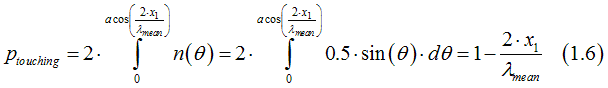
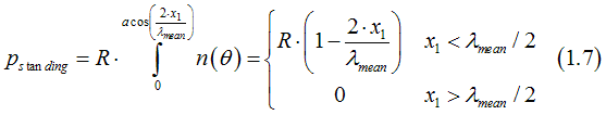
As was mentioned above, the probability that a running-wave electron, which touches the interface, becomes a standing-wave electron is R. Therefore, the number of the standing-wave electrons at point x=x1 is calculated as
It should be noted that in the case of a more realistic Gaussian-shape wave function (Gaussian-shape envelop function), the probability of electron to be a standing-wave electron depends on the amount of overlap of the electron wave function with the regions of the first and second metals
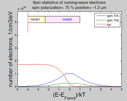
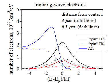
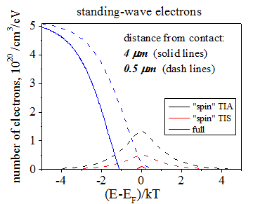
Fig.19. Energy distribution of electrons in vicinity of the interfacefor electrons, which wave vector is normal to interface |
||||
|
||||
|
||||
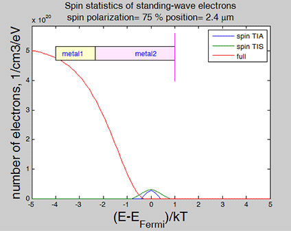
Fig.19. Number of running-wave electrons (left figures) and standing-wave electrons (right figures) in metal 2 at distances 4 mm (solid lines) and 0.5 mm (solid lines) from the contact with metals 1. Black line shows the number of spin- polarized electrons ("spin" TIA). Red line shows the number of spin- unpolarized electrons ("spin" TIS). Blue line shows the number of spin- inactive electrons (full). |
||||
| animated parameter is distance of the electron from interface | ||||
material parameters (click to extend)
It is assumed that there is no defects in metals and the mean-free path is only limited by the quantum contribution The bulk number of electrons: n1=1E19 1/cm3 (metal 1) and n2=1E19 1/cm3 (metal (2). Mean-free path: l um (metal 1) and it equals to 1 um in metal 1 and 2 um ( metal 2). Refractivity of contact R : 0.5 (metal 1) and 0.75 ( metal 2). Spin polarization: 75% (metal 1) ; 75% (metal 2)
|
||||
| Notice: The mean-free-path independent scattering (scatterings on phonon) are ignored. This gives unrealistically large number of standing-wave spin- inactive electrons at lower energy, because of their unrealistically long mean-free path. | ||||
When an electron is passing through a contact, it can be reflected or scattered to become a standing-wave electron. Otherwise, it is passing the contact as a running-wave electron. In the vicinity of a contact, the electron wave function spreads into both metals. As a running-wave electron approaches the contact interface, the more of its wave function penetrates into the second metal making the probability of the electron reflection higher. This is the reason of the continuous decrease of the number of the running-wave electron when the distance to interface decreases. As a running-wave electron moves through the contact interface, the overlap of its wave function with the regions of the first and second metals changes continuously without a step. This literally means that at both sides of the contact the number of the running-wave electrons should be the same or in other words the distribution of the running-wave electrons throughout the contact should be without steps. This condition gives the ratio between contact reflectivity R1 of metal 1 and contact reflectivity R2 of metal 2 as
![]()
where indexes 1 and 2 correspond to metal 1 and metal 2 from sides of the contact.
From Eq. (1.9) the contact refractivity of one side of the contact can be calculated from the refractivity of another side of the contact as
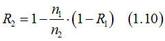
note: Since the contact refractivity R can not be negative, in case of n2 is greater than n1, the contact refractivity of the metal 2 can be only in the interval
for example at a contact between a semiconductor and a metal, the contact refractivity in the metal is very close to 1 and almost all electrons near contact are the standing-wave electrons. In contrast, the contact refractivity in the semiconductor may be from 0 to 1.
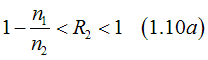
The number of running-wave electrons through the contact can be calculated as
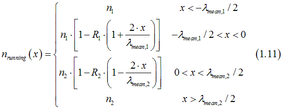
The number of the standing-wave electrons is calculated as
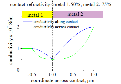
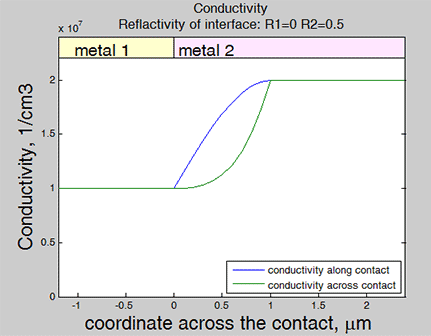
Fig.20. Conductivity of current of running-wave electron in vicinity of contact Mean-free path is the same for all electrons in each metal (incorrect assumption) |
||
|
||
Fig.20. Conductivity in direction perpendicularly to contact (green line) and parallel to contact (blue line) in the vicinity of contact between metal 1 and metal 2. Animated parameter of left figure is the refractivity of the contact. Note1: Figure shows only the conductivity of current of running-wave electrons, it may be a significant additional scattering current in the vicinity of interface material parameters (click to extend)
The metal 1 (left) and metal 2 (right) are contacted at x=0. The bulk conductivity: 1E7 S/m (metal 1) and 2E7 S/m (metal2) Mean-free path: l um (metal 1) and 2 um ( metal 2).
|
Figure 18 shows the distribution of running-wave and standing-wave electrons in the vicinity of a contact between two metals with different numbers of the conduction electrons. At a distances longer than ![]() /2 from the interface all electrons are running-wave electrons. For shorter distances the number of the running-wave electrons decreases becoming smallest at the interface. In contrast, the number of the standing-wave electrons increases becoming largest at the interface.
/2 from the interface all electrons are running-wave electrons. For shorter distances the number of the running-wave electrons decreases becoming smallest at the interface. In contrast, the number of the standing-wave electrons increases becoming largest at the interface.
For calculation of Fig. 18 it is assumed that in each metal the mean-free path is the same for all electrons. However, the mean-free path![]() depends significantly on the electron energy and the type of the state the electron occupies (See here). Figure 19 shows the calculated numbers of spin- polarized and spin- unpolarized conduction electrons at different distances from the interface. The energy dependence of
depends significantly on the electron energy and the type of the state the electron occupies (See here). Figure 19 shows the calculated numbers of spin- polarized and spin- unpolarized conduction electrons at different distances from the interface. The energy dependence of![]() was included into the calculations.
was included into the calculations.
The "full" states are the most affected in the proximity of the contact interface. Even at the long distance of 4 um from the contact there is a significant number of the standing-wave electrons occupying the "full" states at low energy. For a shorter distance of 0.5 um there is a significant number the standing-wave electrons of all types and all energies.
 The conductivity is different for currents flow along and across an interface!!!!
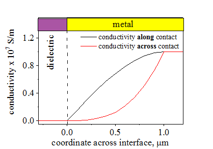
Fig.20(b) Conductivity of current of running-wave electron in vicinity of interface Mean-free path is the same for all electrons in each metal (incorrect assumption) |
|
Fig.20(b).Conductivity in direction perpendicularly to contact (green line) and parallel to contact (blue line) in the vicinity of interface between dielectric and metal. material parameters (click to extend)
The bulk conductivity of metal : 1E7 S/m (metal 1) Mean-free path in metal: l um (metal 1)
|
Currents flow along and across interfaces calculated below. For both cases the current is calculated from Eq. (11.8).
As can be seen from Eq. (1.2) the number of the running -wave electrons depends on the electron moving direction. The closer the moving direction is to the interface normal, the higher the probability for the electron to be the standing-wave type. This makes the conductivity of the running-wave electrons to be anisotropic in the vicinity of a contact. This means that near an interface the conductivity to become different for the currents flowing along and across the interface.
The current that flows perpendicularly to the interface can be calculated from Eq. (11.8) here., where theta is both the angle between the electron movement direction and the normal to the interface and the angle between the electron movement direction and the current direction. From Eq. (1.3) the probability that an electron is of the running-wave type is
Substituting Eq. (1.20) into Eq. (11.8) here. and integrating gives the current flowing perpendicularly to the interface as
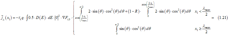
or
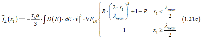

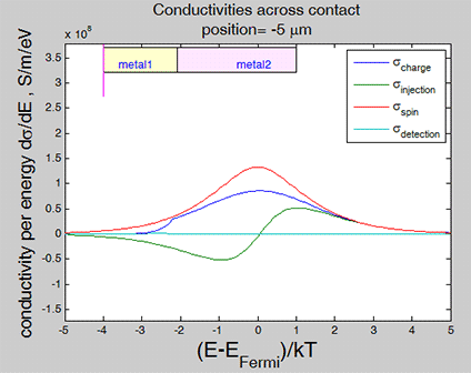
Fig.21. Conductivity in vicinity of contact |
||||||
|
||||||
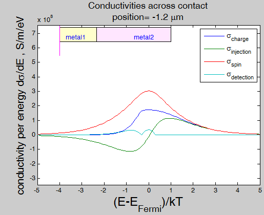
Fig.21. Charge, Spin, Detection and Injection conductivities near contact between metals 1 and 2.. The metal 1 (left) and metal 2 (right) are contacted at x=0. Spin polarization is 45% in both metals. The bulk conductivity of metal 1 and metal 2 is 2E7 S/m and 4E7 S/m, respectively. Notice: The mean-free-path independent scattering (scatterings on phonon) are ignored. Note1: In case when there is no reflectivity in metal1 is zero (R1=0), the reflectivity in metal2 is not zero R2=0.5 material parameters (click to extend)
The metal 1 (left) and metal 2 (right) are contacted at x=0. The bulk conductivity: 1E7 S/m (metal 1) and 2E7 S/m (metal2) The contact refractivities R1=0.5 (metal 1) and R2=0.75 (metal 2) Mean-free path: 1 um (metal 1) and 2 um ( metal 2). Spin polarization: 45 % (both metals)
|
In order to calculate the current flowing along the interface, we use the cylindrical coordinates, where theta is defined as the angle between the electron movement direction and the direction of current flow. Phi is the angle between the normal to the interface and the projection of the electron movement direction into the plane perpendicular to the current flow. Than, the condition that the electron of the running wave-type is
![]()
The range of angles, where condition (1.22) can be satisfied is
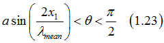
In the region in the vicinity of the interface, where![]() , the current along the interface can be calculated from Eq. (11.8) here, and Eqs. (1.23), (1.22) as
, the current along the interface can be calculated from Eq. (11.8) here, and Eqs. (1.23), (1.22) as
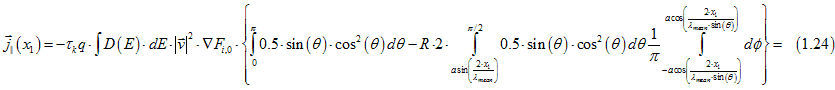
or
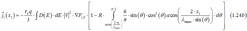
The integrals of Eqs. (1.21b), (1.24b) can be evaluated numerically.
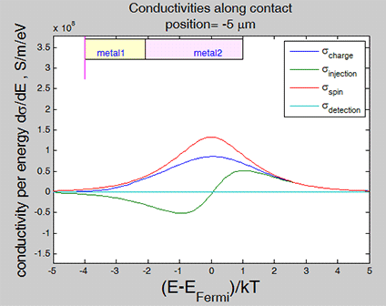
Fig.21. Conductivity in the vicinity of contact |
||
|
||
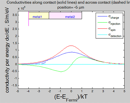
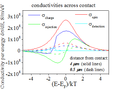
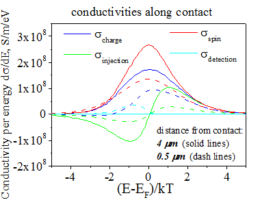
Fig. 21 charge, injection, spin-diffusion and detection conductivities for a current of running-wave electrons flowing (a) along a contact and (b) across a contact. Solid and dash lines correspond to conductivities in metal 2 at distances of 4 um and 0.5 um from contact, respectively. material parameters (click to extend)
The metal 1 (left) and metal 2 (right) are contacted at x=0. The bulk conductivity: 1E7 S/m (metal 1) and 2E7 S/m (metal2) The contact refractivities R1=0.5 (metal 1) and R2=0.75 (metal 2) Mean-free path: 1 um (metal 1) and 2 um ( metal 2). Spin polarization: 45 % (both metals)
|
Figure 20 shows the conductivity of the current of the running-wave electrons in the vicinity of a contact between two metals and a contact between a metal and a dielectric. Through the contact the conductivity decreases from the value of the bulk conductivity of metal 1, reaches a minimum at the contact interface and then increases to the value of the bulk conductivity of metal 2. In the case when the reflectivity R of the contact is 1 (for example, a metal-dielectric contact (Fig.20 (b))), at the contact interface the conductivity of the current of the running-wave electrons becomes zero and the scattering current becomes only the remaining transport mechanism. It is the case, for example, of transport through a tunnel junction. The reduction of the conductivity occurs in each metal within ![]() /2. The conductivity for a current across the interface decreases sharper than for a current along the interface.
/2. The conductivity for a current across the interface decreases sharper than for a current along the interface.
For the calculation of Fig. 20 it is assumed that in each metal the mean-free path is the same for all electrons. As was explained above, it is necessary to include in calculation the dependence of ![]() on the electron energy and on the type of state, which the electron occupies. Figure 21 shows the charge, injection, spin-diffusion and detection conductivities at different distance from the contact. Since the density of states may be different for the metals at the sides of the contact, the state conductivities can not describe the change of the conductivity through contact. Instead the derivation of the conductivities
on the electron energy and on the type of state, which the electron occupies. Figure 21 shows the charge, injection, spin-diffusion and detection conductivities at different distance from the contact. Since the density of states may be different for the metals at the sides of the contact, the state conductivities can not describe the change of the conductivity through contact. Instead the derivation of the conductivities ![]() has been used in Fig.21. The conductivities can be calculated as
has been used in Fig.21. The conductivities can be calculated as
 Conclusions
(1) As closer position of an electron to interface, the higher possibility for the electron to be a standing-wave electron (Fig.3)
 (2) The largest number of standing-wave electrons occupies the "full" state with low energy and "spin" TIA states near the Fermi energy, because of the long mean-free path of these states. (Fig.3)
note: in calculation of Figs.3,4 the mean-free-path independent scattering (scatterings on phonon) are ignored. This gives unrealistically large number of standing-wave "full" states at lower energy, because of unrealistically long mean-free path.
(3) Charge conductivity decreases. Therefore in the vicinity of an interface the conductivity is always lower than that in the bulk of a metal (the contact resistance). The most affected is the running-wave conductivity conductivity of the "full" states.
(4) The injection state conductivity is still asymmetric as the function of the energy. Therefore, in the case of a metal the injection conductivity is not large. However, it is not fully asymmetric and even for the metal with constant density of the state, the injection conductivity can be non-zero (Fig.4(center)).
(6) The spin conductivity decreases in the vicinity of the interface
 (7) The detection conductivity becomes non-zero in the vicinity of the contact.
Note1: the detection conductivity is zero in the bulk of semiconductors and metals
In contrast to the bulk, where there is no scattering conductivity or the scattering conductivity is small, near an interface the scattering conductivity becomes substantial.
![]() The tunneling through a tunnel barrier or a Schottky barrier are examples of the scattering conductivity through the interface.
The tunneling through a tunnel barrier or a Schottky barrier are examples of the scattering conductivity through the interface.
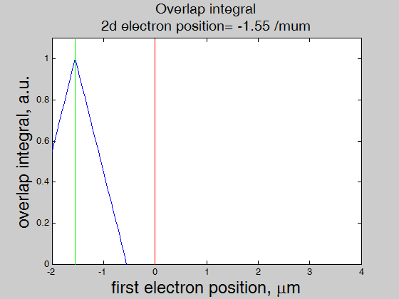
The scattering conductivity is due to scatterings from one quantum state to another quantum state. The scattering probability from one quantum state to another quantum state is linearly proportional to the overlap integral of the wave functions of two states. Below the overlap integral is calculated.
(1) The approximation of the square-shape wave function is used.
(2) Both running-wave electrons and standing-wave electrons contribute to the scattering conductivity. Below it is assumed that a standing-wave and a running-way electron contributes equally to the scattering conductivity.
(3) A contact between two metals, which are only different by their different mean-free paths, is calculated. In a realistic contact the densities of the states in metals are different as well. The inclusion this difference into the calculations is straightforward.
Scattering in the bulk
Within the approximation of square-shape wave function, in bulk the wave function of an electron, which moves along the x-axis and which center at time t=to is at point x0, is calculated as
From Eq. (3.1) the overlap integral between wave functions of two electrons, which centers are at points x0 and x0+delta_x (delta_x>0), is calculated as
and the overlap integral for electrons at points x0 and x0-delta_x (delta_x>0), is calculated as
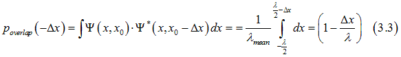
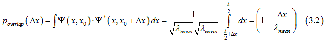
Eqs. (3.2) and (3.3) can be combined for any sign of delta_x as
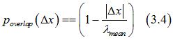
From Eq. (3.4) in the bulk the probabilities for electron to be scattered backward and forward are the same. This a reason there is no scattering current in the bulk for the running wave electrons..
 |
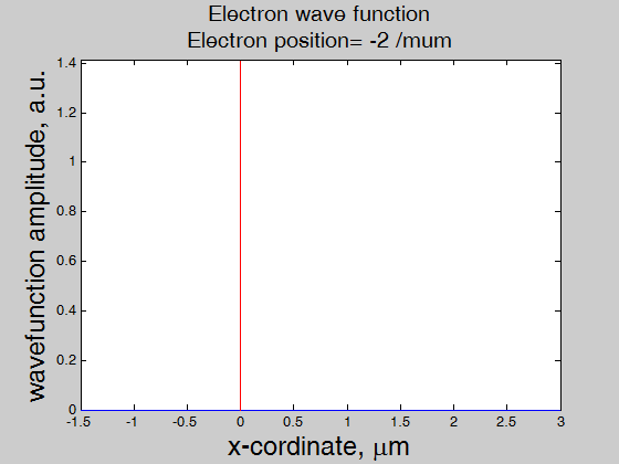 |
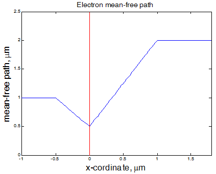
Fig.5 The electron mean-free path in the vicinity of the interface between two metals. The interface is at x=0 (red line). The mean-free path in bulk of metal 1 (left) and metal 2 (right) is 1 um and 2 um. The mean-free path at the interface is 1 um. |
Fig.6, The wave function of an electron as the electron passes through the interface. The interface is at x=0 (red line). The green line shows the center position of the electron. Note: near interface the amplitude of the wave function increases because of the shorter mean-free path. |
The wave function is continuous through the interface. It is assumed that even an wave function extended over interface keeps its square shape.
A simplest contact between two is calculated, where only difference between the metals is different value of the mean-free path.
Near an interface an electron can be scattered on imperfections of the interface. Therefore. the electron mean-free path is shortest near interface. Depending on the electron position x0, the mean-free path can be calculated as
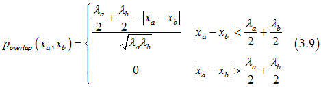
The overlap integral between the wave functions (Eq.(3.1) of two electrons at positions x0=x_a and x0=x_b (x_b> x_a) is calculated as
 |
|
Fig.5 The electron mean-free path in the vicinity of the interface between two metals. The interface is at x=0 (red line). The mean-free path in bulk of metal 1 (left) and metal 2 (right) is 1 um and 2 um. The mean-free path at the interface is 1 um. |
Fig.6, The wave function of an electron as the electron passes through the interface. The interface is at x=0 (red line). The green line shows the center position of the electron. Note: near interface the amplitude of the wave function increases because of the shorter mean-free path. |
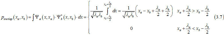
in the case when x_a> x_b

Combining Eqs.(3.7) and (3.8), we have
.
I will try to answer your questions as soon as possible