Dr. Vadym Zayets
v.zayets(at)gmail.com
My Research and Inventions
click here to see all content |

Dr. Vadym Zayetsv.zayets(at)gmail.com |
|
|
more Chapters on this topic:IntroductionTransport Eqs.Spin Proximity/ Spin InjectionSpin DetectionBoltzmann Eqs.Band currentScattering currentMean-free pathCurrent near InterfaceOrdinary Hall effectAnomalous Hall effect, AMR effectSpin-Orbit interactionSpin Hall effectNon-local Spin DetectionLandau -Lifshitz equationExchange interactionsp-d exchange interactionCoercive fieldPerpendicular magnetic anisotropy (PMA)Voltage- controlled magnetism (VCMA effect)All-metal transistorSpin-orbit torque (SO torque)What is a hole?spin polarizationCharge accumulationMgO-based MTJMagneto-opticsSpin vs Orbital momentWhat is the Spin?model comparisonQuestions & AnswersEB nanotechnologyReticle 11
more Chapters on this topic:IntroductionTransport Eqs.Spin Proximity/ Spin InjectionSpin DetectionBoltzmann Eqs.Band currentScattering currentMean-free pathCurrent near InterfaceOrdinary Hall effectAnomalous Hall effect, AMR effectSpin-Orbit interactionSpin Hall effectNon-local Spin DetectionLandau -Lifshitz equationExchange interactionsp-d exchange interactionCoercive fieldPerpendicular magnetic anisotropy (PMA)Voltage- controlled magnetism (VCMA effect)All-metal transistorSpin-orbit torque (SO torque)What is a hole?spin polarizationCharge accumulationMgO-based MTJMagneto-opticsSpin vs Orbital momentWhat is the Spin?model comparisonQuestions & AnswersEB nanotechnologyReticle 11
more Chapters on this topic:IntroductionScatteringsSpin-polarized/ unpolarized electronsSpin statisticselectron gas in Magnetic FieldFerromagnetic metalsSpin TorqueSpin-Torque CurrentSpin-Transfer TorqueQuantum Nature of SpinQuestions & Answers
more Chapters on this topic:IntroductionTransport Eqs.Spin Proximity/ Spin InjectionSpin DetectionBoltzmann Eqs.Band currentScattering currentMean-free pathCurrent near InterfaceOrdinary Hall effectAnomalous Hall effect, AMR effectSpin-Orbit interactionSpin Hall effectNon-local Spin DetectionLandau -Lifshitz equationExchange interactionsp-d exchange interactionCoercive fieldPerpendicular magnetic anisotropy (PMA)Voltage- controlled magnetism (VCMA effect)All-metal transistorSpin-orbit torque (SO torque)What is a hole?spin polarizationCharge accumulationMgO-based MTJMagneto-opticsSpin vs Orbital momentWhat is the Spin?model comparisonQuestions & AnswersEB nanotechnologyReticle 11
more Chapters on this topic:IntroductionTransport Eqs.Spin Proximity/ Spin InjectionSpin DetectionBoltzmann Eqs.Band currentScattering currentMean-free pathCurrent near InterfaceOrdinary Hall effectAnomalous Hall effect, AMR effectSpin-Orbit interactionSpin Hall effectNon-local Spin DetectionLandau -Lifshitz equationExchange interactionsp-d exchange interactionCoercive fieldPerpendicular magnetic anisotropy (PMA)Voltage- controlled magnetism (VCMA effect)All-metal transistorSpin-orbit torque (SO torque)What is a hole?spin polarizationCharge accumulationMgO-based MTJMagneto-opticsSpin vs Orbital momentWhat is the Spin?model comparisonQuestions & AnswersEB nanotechnologyReticle 11
more Chapters on this topic:IntroductionTransport Eqs.Spin Proximity/ Spin InjectionSpin DetectionBoltzmann Eqs.Band currentScattering currentMean-free pathCurrent near InterfaceOrdinary Hall effectAnomalous Hall effect, AMR effectSpin-Orbit interactionSpin Hall effectNon-local Spin DetectionLandau -Lifshitz equationExchange interactionsp-d exchange interactionCoercive fieldPerpendicular magnetic anisotropy (PMA)Voltage- controlled magnetism (VCMA effect)All-metal transistorSpin-orbit torque (SO torque)What is a hole?spin polarizationCharge accumulationMgO-based MTJMagneto-opticsSpin vs Orbital momentWhat is the Spin?model comparisonQuestions & AnswersEB nanotechnologyReticle 11
|
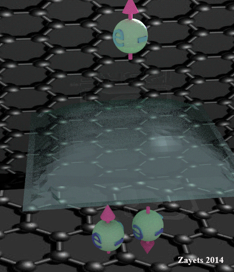
Mean-Free Path. Bulk conductivity of a metal with defects.
Spin and Charge TransportThe mean-free path is average distance an electron passes between scatterings. The mean-free path is also the effective length of the wavefunction of delocalized electrons.The influence of the mean-free path on transport becomes substantial in two cases. The first case is when the mean-free path becomes comparable to the average distance between defects. The second case is when an electron distance from an interface is comparable or less than the mean-free path. In both cases the number of running-wave electrons decreases and the number of standing-wave electrons increases. As a consequence, the conductivity reduces and importantly the spin properties of the conductivity are significantly modified. The detection conductivity becomes non-zero and the injection conductivity becomes larger.
|
| Mean-free path | ||||||
|---|---|---|---|---|---|---|
|
Results in short
I. The length of the mean-free path significantly depends on the electron energy.
Charge, injection,detection and spin-diffusion state conductivities |
||||
|
2.Because of defects, the number of standing-wave electrons increases and the number of the running-wave electron decreases.
3. The probability for an electron to become a standing-wave electrons become higher when
a) distance between defects become shorter
b) mean-free path becomes longer
4. The number of standing-wave electrons depends on the electron energy and the type of the state the electron occupies. There are significant number of standing electrons occupying:
a) "full" states at energies lower than the Fermi energy.
b) "spin" states of the TIA assembly at energies near the Fermi energy.


7. It might be possible that the spin properties of a metal can be engineered by fabricating artificial defects inside the metal with an optimized distribution.

The mean-free path is the distance through which an electron moves between scatterings. 
Since an electron is a wave package, the mean-free path can be considered the effective width of this electron wave package or an effective size of an electron or the effective length within which the electron interacts with defects, phonons and other inhomogeneities.
In case of a larger number of scatterings, the mean-free path becomes.

Fig.4. Length of photon Emission of photon by an excited atomA photon is emitted only between two subsequent colliding or scattering of the excited atom. Next, another photon is emitted. The length of the photon is determined by time between two subsequent scatterings of the excited atom. Similarly the effective length of an electron is determined by time between two subsequent scatterings of the electron. |
|
| Click on image to enlarge it or here for a middle size |
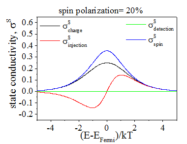
A. There are two distinguished differences between conductivities in conductors with and without defects. The first difference is the value of the detection conductivity ![]() . It is zero in a conductor without defects for any electron energy and it is non-zero in a conductor with defects at energies near the Fermi energy. The second difference is the dependence of the charge (conventional) conductivity
. It is zero in a conductor without defects for any electron energy and it is non-zero in a conductor with defects at energies near the Fermi energy. The second difference is the dependence of the charge (conventional) conductivity ![]() on the spin polarization sp of the electron gas. The charge conductivity is independent of the spin polarization in a conductor without defects. This means that there is no magneto-resistance effect in a conductor without defects. In contrast, in a conductor with defects, the charge conductivity is dependent on the spin polarization of the electron gas and there is a magneto-resistance effect. The conduction of electrons of only energies near the Fermi energy depends on the spin polarization. Therefore, this magneto-resistance effect may exists only in a metal, but not in a non-degenerate semiconductor.
on the spin polarization sp of the electron gas. The charge conductivity is independent of the spin polarization in a conductor without defects. This means that there is no magneto-resistance effect in a conductor without defects. In contrast, in a conductor with defects, the charge conductivity is dependent on the spin polarization of the electron gas and there is a magneto-resistance effect. The conduction of electrons of only energies near the Fermi energy depends on the spin polarization. Therefore, this magneto-resistance effect may exists only in a metal, but not in a non-degenerate semiconductor.
In the bulk of a conductor without defects a spin diffusion current flows without any charge diffusion current. Such spin current is possible only because in the bulk of a conductor without defects there is a balance. The numbers of spin-polarized and spin-unpolarized electrons, which diffuse in the opposite directions along the gradient of the spin accumulation, are exactly equal. This results in a spin current without any charge accumulation and ![]() =0. In a conductor with defects the number of the running-wave electrons in “full” states of the TIS assembly (spin-unpolarized electrons) becomes substantially smaller at lower energies. The number of the running-wave electrons in the “spin” states of the TIA assembly (spin-polarized electrons) becomes smaller at the Fermi energy. This unbalances the number of spin-polarized and spin–unpolarized electrons, which diffuse in opposite directions. As a result, the charge is accumulated along the spin diffusion and
=0. In a conductor with defects the number of the running-wave electrons in “full” states of the TIS assembly (spin-unpolarized electrons) becomes substantially smaller at lower energies. The number of the running-wave electrons in the “spin” states of the TIA assembly (spin-polarized electrons) becomes smaller at the Fermi energy. This unbalances the number of spin-polarized and spin–unpolarized electrons, which diffuse in opposite directions. As a result, the charge is accumulated along the spin diffusion and ![]() .
.
In a conductor without defects, all electrons are running-wave electrons. When the spin polarization of the electron gas changes, the numbers of spin-polarized and spin-unpolarized electrons change. However, the total number of the running-wave electrons remains constant and the charge conductivity remains unchangeable. In a conductor with defects the ratio of the standing-wave to running-wave electrons is different for the TIS and TIA assemblies. This means that when the spin polarization of the electron gas changes, the total number of the running-wave electrons changes. As a consequence, the conductivity of the running-wave electrons become dependent on the spin polarization of the electron gas.
The mean free path is finite, because an electron experiences scatterings

 |
| Fig. 1. The Quantum contribution into the mean-free path. Even the electron has non-zero speed, it can not move into neighbor states, because the state is already occupied by two electrons of opposite spins. In this case the electron can not be scattered and the mean-free-path become long. |
The Quantum contribution describes the fact that an electron can be scattered only when there is an unoccupied neighbor state where the electron can be scattered to (See Fig.1). 
The mean-free-path-dependent scattering is due a scattering centers which have a defined position in the space (for example, the scattering on defects and dislocations).
The mean-free-path-independent scattering is due a scattering centers which do not have a defined position in the space (for example, the scatterings on phonons). Also, the scattering on defects contribute on this scattering, because an electron has non-zero speed and even if electron mean-free-path is very short, the electron can reach the defect and be scattered after some time.
Three mechanisms, which influence ![]() , can be distinguished. The first mechanism is the quantum-mechanical limitation for a scattering. An electron is a fermion and it can be scattered only if there is an unoccupied state where the electron can be scattered into. In The second mechanism is the mean-free-path-dependent scattering. This is the scattering on defects and dislocations, which have some spatial distribution with some average distance between them. When mean is significantly smaller than this distance, the scattering probability is small, but when mean is comparable or longer than the average distance between defects, the scattering probability becomes larger. The third mechanism is the mean-free-path-independent scattering. This is the scattering on phonons and magnons, which does not depend on mean. the mean-free path mean. can be calculated as
, can be distinguished. The first mechanism is the quantum-mechanical limitation for a scattering. An electron is a fermion and it can be scattered only if there is an unoccupied state where the electron can be scattered into. In The second mechanism is the mean-free-path-dependent scattering. This is the scattering on defects and dislocations, which have some spatial distribution with some average distance between them. When mean is significantly smaller than this distance, the scattering probability is small, but when mean is comparable or longer than the average distance between defects, the scattering probability becomes larger. The third mechanism is the mean-free-path-independent scattering. This is the scattering on phonons and magnons, which does not depend on mean. the mean-free path mean. can be calculated as
Combining these three contributions, the mean-free-path ![]() can be calculated as
can be calculated as
where ![]() is the probability that there is an available unoccupied states into which an electron can be scattered,
is the probability that there is an available unoccupied states into which an electron can be scattered, ![]() is the scattering probability, which is independent on the mean free path;
is the scattering probability, which is independent on the mean free path; ![]() is the scattering probability, which is independent on the mean free path.;
is the scattering probability, which is independent on the mean free path.; ![]() is mean free path when there is no mean-free-path dependent scatterings and there is a sufficient number states in which an electron can be scattered into
is mean free path when there is no mean-free-path dependent scatterings and there is a sufficient number states in which an electron can be scattered into
![]()
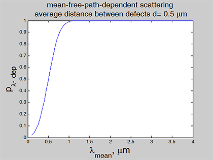
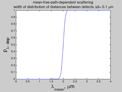
Mean-free-path-dependent scattering
he distribution of the defects in a metal depends on the metal fabrication method. The normal or Gaussian distribution of defects is the most probable. In this case the probability, that the distance from one defect to the closest neighbor defect equals d, can be calculated as

Where d_0 is the average distance between defects and delta_d is the width of the distribution.
Normalizing the distribution (1.3)
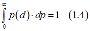
we obtain
probability |
||||
material parameters (click to extend)
Fig. 3(a) The width of distribution of distances between defect delta_d=0.3 um Fig. 3(b) The average distance between defect d=2 um |

We can assume that an electron can be scattered only if its wave function overlap at least one defect at any time. Therefore, an electron is scattered only if its mean-free path is shorter than the distance between defects. Then, the scattering probability ![]() is calculated as
is calculated as

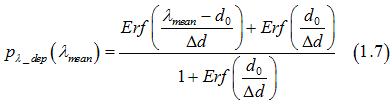
Integrating Eq. (1.6) the probability ![]() of the mean-free-path-dependent scattering is obtained as
of the mean-free-path-dependent scattering is obtained as
mean-free path
|
|||
|
|||
Fig.4. The mean-free path
|
The Quantum contribution describes the fact that an electron can be scattered only when there is a place where to be scattered to (See Fig.1) .
The electron from a "full" state can be scattered either into "empty" state or "spin" state. The probability that near a "full" state there is "empty" state or "spin" states. Since such probabilities described by the distributions functions, the ![]() for "full" states is calculated as:
for "full" states is calculated as:
![]()
where ![]() are distribution functions for the "spin" states of the TIA assembly, the "spin" states of the TIS assembly and "empty" states
are distribution functions for the "spin" states of the TIA assembly, the "spin" states of the TIS assembly and "empty" states
The electron from a "spin" state can be scattered either into "empty" state or another "spin" state. Also, an electron from a "full" state can be scattered into the "spin" state.
The electron spin influences the scattering from one "spin" state to another "spin" state. For example, all electrons of the TIA assembly have the same spin direction and an electron can not be scattered from one "spin" state. In contrast, the electron can be scattered into a "spin" state of the TIS assembly, because spin direction of this "spin" state can any direction with equal probability. Therefore, he ![]() for "spin" states of TIA assembly is calculated as:
for "spin" states of TIA assembly is calculated as:
An electron from a "spin" state of the TIS assembly can be scattered into a "empty" state or an electron from a "full" state can be scattered into the "spin" state or "spin" states of the TIA assembly or "spin" states of the TIS assembly. Therefore, he ![]() for "spin" states of TIS assembly is calculated as:
for "spin" states of TIS assembly is calculated as:
mean-free path
|
|||
|
|||
Fig.4. The mean-free path material parameters (click to extend)
The width of distribution of distances between defect delta_d=0.3 um The average distance between defect d=2 um Reflectivity of a defect R_d= 0.8 Ration of mean-free-path dependent to mean-free-path independent scatterings p_dependent/p_independent
|
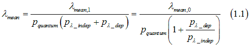
The mean-free path ![]() is calculated from Eq.(1.1) using Eqs. (1.7-1.10)
is calculated from Eq.(1.1) using Eqs. (1.7-1.10)
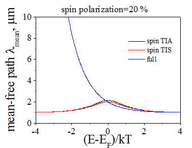
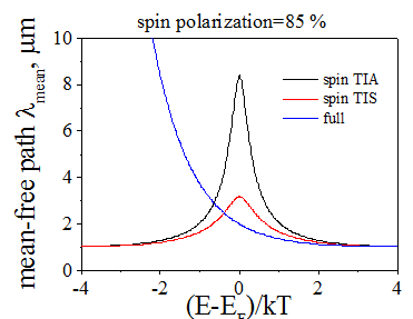
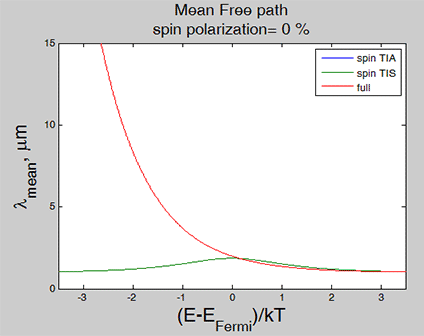
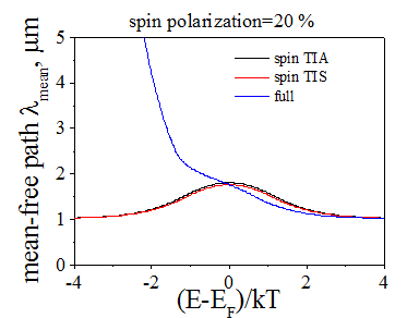
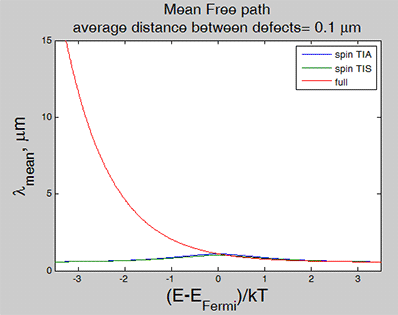
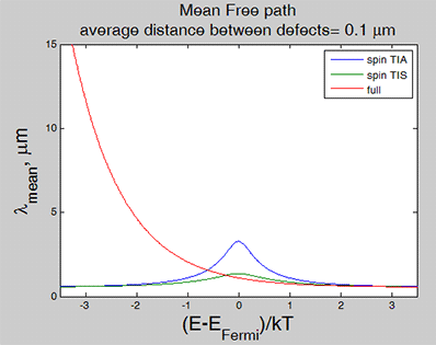
Figs.4-7 shows calculated mean-free path ![]() as the function of an electron energy. In all figures, when it was not mentioned, the spin polarization is 50%, the average distance between defects d is 2 um, the width of the distribution of the distances between defects delta_d is 0.3 um,
as the function of an electron energy. In all figures, when it was not mentioned, the spin polarization is 50%, the average distance between defects d is 2 um, the width of the distribution of the distances between defects delta_d is 0.3 um, ![]() is 1 um (See Eq.(1.1) ) , the ratio of probabilities of
is 1 um (See Eq.(1.1) ) , the ratio of probabilities of ![]() -dependent to
-dependent to ![]() -independent scatterings
-independent scatterings  is 80 %.

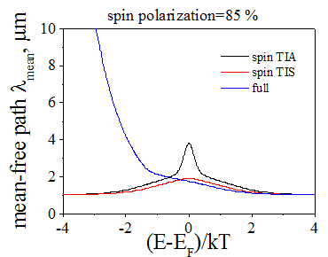
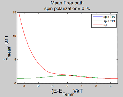
1) The mean-free path significantly depends on the electron energy, spin polarization of a metal and the defect distribution in the metal.
2) Below the Fermi energy the mean-free path of "full" states is very long. For example, 3kT below the Fermi energy the mean-free-path of "full" states may be 15 times longer than that at the Fermi energy.
3) The length of the mean-free path of "spin" states of the TIA assembly significantly increase near the Fermi energy with increasing of the spin polarization sp of metal. It can be 10 times larger than the length of the mean-free path of "spin" states of the TIA assembly at spin polarization larger than 90 %.
Running waves |
Standing waves |
|
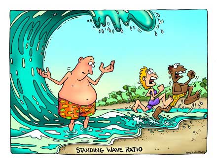 |
| The running-wave electrons are moving in the space. They can be scattered. Therefore, these electrons contributes to both conductivities | Fig. The quantum mechanic does not require that an object with non-zero speed necessary moves in the space. One example is a standing wave, which has non-zero speed, does not move in the space. A standing wave can be decomposed as a sum of two waves running in opposite directions. The standing-wave electrons contribute only to the scattering conductivity. |
Note: In bulk of a metal, the major electron transport mechanism is running-wave conduction. This conduction is proportional to the number of the running-wave electrons in the metal..
Note: As the number of defects, dislocations and phase boundaries in a metal increases, the number of the running-wave electrons decreases and the number of the standing-wave electrons increases.
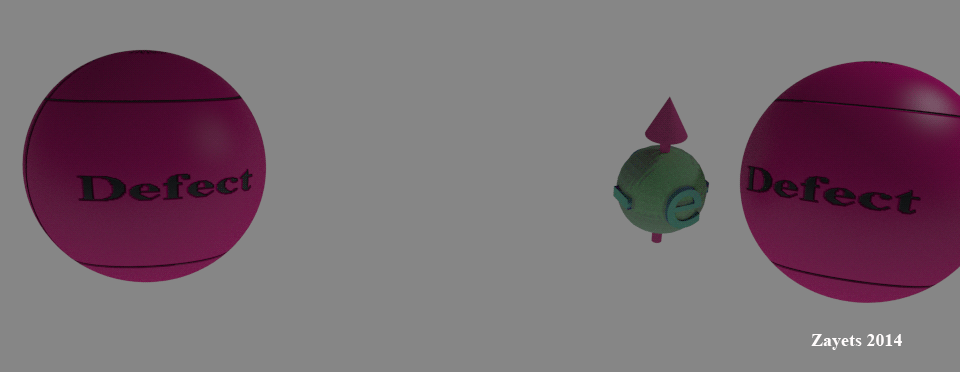
A standing-wave electron. An example, an electron bouncing between two defects. |
|
Note: An electron can bound to only one defect making a standing wave electronNote: An electron can bound to an interface making a standing wave electron |
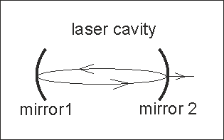
Standing-wave photon in laser cavity |
|
Photon is reflecting back and forward between two mirrors forming a standing wave. When the photon passes through the semitransparent mirror, it becomes the running-wave photon. Similarly, a standing-wave electron is reflected between two defects (note, only one defect is sufficient to make a standing wave electron) |
The ![]() -depending scatterings are scatterings from defects, which have defined position in space or standing centers. Therefore, the number of standing-wave in a metal should be proportional to the ratio of probability of
-depending scatterings are scatterings from defects, which have defined position in space or standing centers. Therefore, the number of standing-wave in a metal should be proportional to the ratio of probability of ![]() -dependent scattering to probability of all types of scatterings. It should be notice that it is not always the scattering on a defect causes forming of a standing-wave electron. We the defect refractivity R_d as a probability that an electron will be a standing-wave electron after a scattering on the defect. Therefore, the ratio of the standing wave (SW) electrons to all electrons (standing-wave electrons(SW) + running wave (RW)) in metal can be calculated as
-dependent scattering to probability of all types of scatterings. It should be notice that it is not always the scattering on a defect causes forming of a standing-wave electron. We the defect refractivity R_d as a probability that an electron will be a standing-wave electron after a scattering on the defect. Therefore, the ratio of the standing wave (SW) electrons to all electrons (standing-wave electrons(SW) + running wave (RW)) in metal can be calculated as
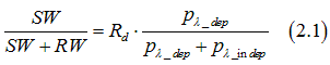
![]() is the scattering probability, which is independent on the mean free path;
is the scattering probability, which is independent on the mean free path; ![]() is the scattering probability, which is independent on the mean free path (See Eq.(1.1) )
is the scattering probability, which is independent on the mean free path (See Eq.(1.1) )
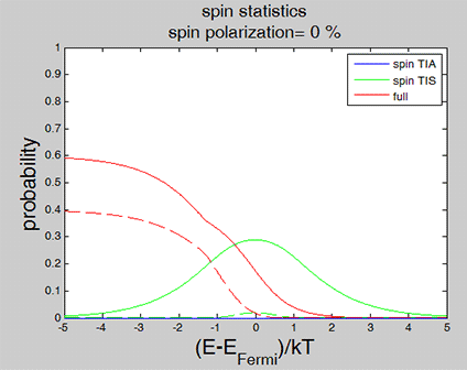
Spin statistic for running-wave electron (solid lines) and standing-wave electrons (dash line) |
||
|
||
Fig.9. Solid lines show the distribution of the running-wave electrons (RW). Dashed lines show the distribution of the standing-wave electrons (SW). Animated parameter is the spin polarization of the metal
material parameters (click to extend)
The width of distribution of distances between defect delta_d=0.3 um The average distance between defect d=2 um Reflectivity of a defect R_d= 0.8 Ration of mean-free-path dependent to mean-free-path independent scatterings p_dependent/p_independent
|
The conclusions from Fig. 11.
(2) There is a significant number of standing-wave electrons for "spin" states of the TIA assembly at energies near the Fermi energy at the spin
(3) The distribution functions become less monotonic with some local peaks.
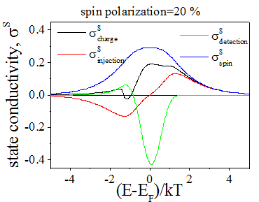
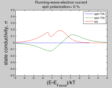
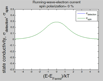
State conductivities for current of running-wave-electrons in the bulk of conductor with defects.Animated parameter is the spin polarization of the metalFor the case without defects See here
|
||||||||
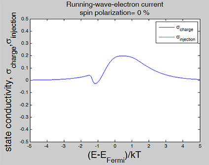
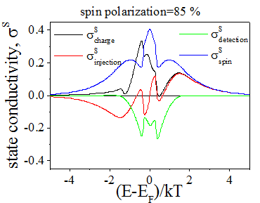
Charge, injection,detection and spin-diffusion conductivities in the bulk of conductor with defects.
material parameters (click to extend)
The width of distribution of distances between defect delta_d=0.3 um The average distance between defect d=2 um Reflectivity of a defect R_d= 0.8 Ration of mean-free-path dependent to mean-free-path independent scatterings p_dependent/p_independent
|
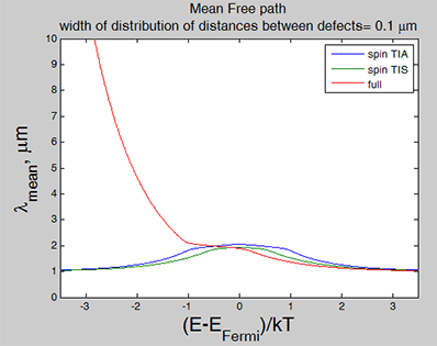
Dependence on the distance between defects
mean-free path.Animated parameter: average distance between defects d. |
||||
material parameters (click to extend)
The width of distribution of distances between defect delta_d=0.3 um The average distance between defect d=2 um Reflectivity of a defect R_d= 0.8 Ration of mean-free-path dependent to mean-free-path independent scatterings p_dependent/p_independent
|
||||
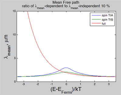
mean-free pathon the scattering parameters |
||||
material parameters (click to extend)
The width of distribution of distances between defect delta_d=0.3 um The average distance between defect d=2 um Reflectivity of a defect R_d= 0.8 Ration of mean-free-path dependent to mean-free-path independent scatterings p_dependent/p_independent
|
||||
 Engineering the spin properties of a conductor
It should be noted that the values of the detection conductivity, the injection conductivity and the magneto-resistance depend on a defect distribution. Materials having the larger detection conductivity or/and the larger injection conductivity or/and the larger magneto-resistance are required for a variety of the practical applications. It might be possible that the spin properties of a metal can be engineered by fabricating artificial defects inside the metal with an optimized distribution. A similar technique was proved to be effective in the case of a photonic crystal, where the optical properties of the crystal can be engineered by inserting artificial defects into the crystal.
 |
| Normal or Strange? |
 However, in an electron gas the electrons diffuses from regions of higher electron concentration to regions of lower electron concentration. It might not be the direction from "-" potential to "+" potential

The flow of electrons along an electrical field form "-" potential to "+" potential.
In this case the charge conductivity ![]() is positive.
is positive.

The flow of electrons along an electrical field form "+" potential to "-" potential.
In this case the charge conductivity ![]() is negative.
is negative.
 Note: in total the electron current should be always normal. Only a current of some type of electrons or a current of electrons of some energy may be strange. For example, the current of "spin" states in the hole current of the running-wave electrons.
 Examples of the strange currents
1. The current of "spin" states with energies below the Fermi energy.
Even though the "spin" states are negatively charged, they diffuse from "+" source to "-" drain
However, the total current (the hole current), which consists of the current of the "spin" states plus the current of the "full" states, is the normal current. It transport the negative charge from from "-" source to "+" drain
I will try to answer your questions as soon as possible

 =1
=1


 The charge conductivity depends on spin polarization sp. There is a Magneto-Resistance effect in the bulk of a metal!!!! (AMR, GMR effects).
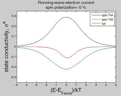