Dr. Vadym Zayets
v.zayets(at)gmail.com
My Research and Inventions
click here to see all content |

Dr. Vadym Zayetsv.zayets(at)gmail.com |
|
|
more Chapters on this topic:IntroductionTransport Eqs.Spin Proximity/ Spin InjectionSpin DetectionBoltzmann Eqs.Band currentScattering currentMean-free pathCurrent near InterfaceOrdinary Hall effectAnomalous Hall effect, AMR effectSpin-Orbit interactionSpin Hall effectNon-local Spin DetectionLandau -Lifshitz equationExchange interactionsp-d exchange interactionCoercive fieldPerpendicular magnetic anisotropy (PMA)Voltage- controlled magnetism (VCMA effect)All-metal transistorSpin-orbit torque (SO torque)What is a hole?spin polarizationCharge accumulationMgO-based MTJMagneto-opticsSpin vs Orbital momentWhat is the Spin?model comparisonQuestions & AnswersEB nanotechnologyReticle 11
more Chapters on this topic:IntroductionTransport Eqs.Spin Proximity/ Spin InjectionSpin DetectionBoltzmann Eqs.Band currentScattering currentMean-free pathCurrent near InterfaceOrdinary Hall effectAnomalous Hall effect, AMR effectSpin-Orbit interactionSpin Hall effectNon-local Spin DetectionLandau -Lifshitz equationExchange interactionsp-d exchange interactionCoercive fieldPerpendicular magnetic anisotropy (PMA)Voltage- controlled magnetism (VCMA effect)All-metal transistorSpin-orbit torque (SO torque)What is a hole?spin polarizationCharge accumulationMgO-based MTJMagneto-opticsSpin vs Orbital momentWhat is the Spin?model comparisonQuestions & AnswersEB nanotechnologyReticle 11
|
All-Metal Transistor. Spin transistor Spin and Charge TransportAbstract:An all-metal transistor, which eliminates the need for semiconductor materials, offers potential advantages such as reduced power consumption, lower operating voltage, and further size scaling. This type of transistor is particularly suited for 3D integration. With its implementation, electronic devices could become both smaller and more versatile.
|
Electronic device (terminator) made of only metals |
 |
Terminator 2: science-fiction movie |
| click on image to enlarge it |
![]() (merit 1): Eliminating the need for high crystal quality:
(merit 1): Eliminating the need for high crystal quality:
In semiconductor-based transistors, crystal periodicity is crucial as it creates the band gap necessary for operation. Maintaining high crystal quality becomes challenging in 3D integration due to the complexities of multi-layer fabrication. In contrast, the proposed all-metal transistor can be fabricated from polycrystalline or amorphous materials, which retain their quality over multiple layers, making them more suitable for 3D integration.
![]() (merit 2): Size downscaling:
(merit 2): Size downscaling:
Traditional Si-based MOSFET transistors are approaching their physical downscaling limits. The proposed transistor, however, is constrained only by the minimum size of its magnetic domains, which can be as small as a few nanometers. Furthermore, as the size of the electrodes and magnetic domains decrease, the On/Off ratio of the transistor improves. This enhanced performance with smaller dimensions makes it ideal for further size reduction and integration into dense 3D architectures.
![]() (merit 3): Lower operating voltage, reduced power consumption and the ability to withstand a high current.
(merit 3): Lower operating voltage, reduced power consumption and the ability to withstand a high current.
Semiconductor transistors operate at voltages near the material’s band gap. For example, Si has a band gap of 1.1 eV, resulting in operating voltages around 1 V. This relatively high voltage limits power consumption reduction in semiconductor transistors. In contrast, the proposed all-metal transistor, which does not rely on a band gap, can operate at much lower voltages, leading to lower power consumption and the ability to handle higher current without performance degradation.
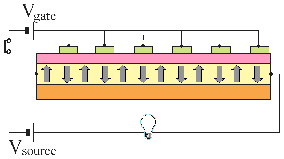
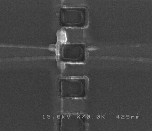
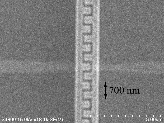
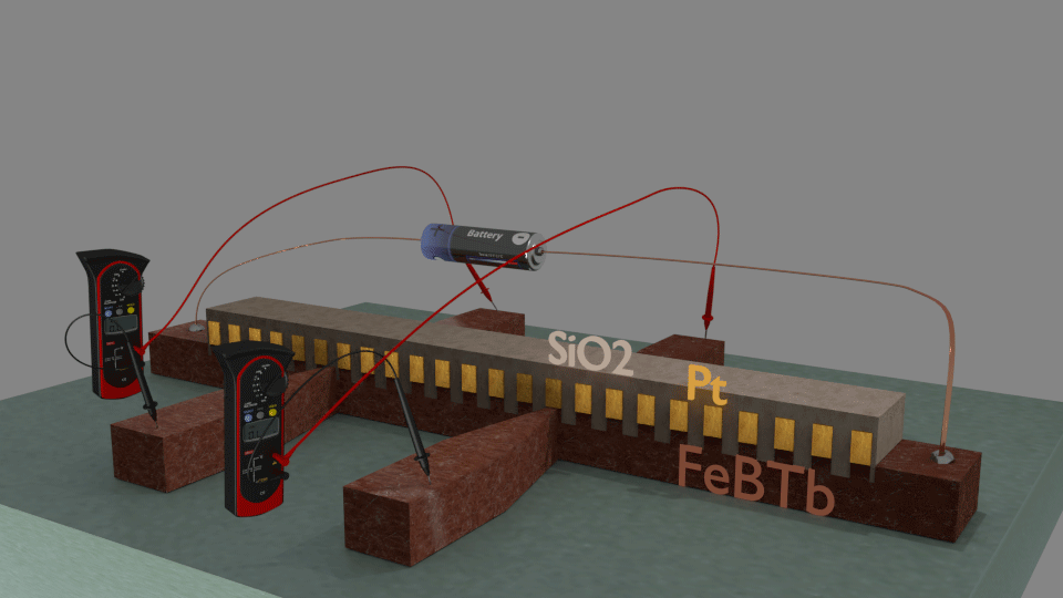
FeBTb nanowire with Pt periodic electrode. |
 |
Periodic Pt electrodes on a ferromagnetic nanowire, which induces the periodical PMA in the wire. The front Hall probe contacts the region under the Pt electrode. The back Hall probe contacts the region in the gap between Pt electrode. Check below for the explanations. click on image to enlarge it |
![]() (reason 1) Simplified Materials and Fabrication.
(reason 1) Simplified Materials and Fabrication.
The all-metal transistor can be fabricated using only metal and dielectric materials, without the need for semiconductors. This allows for the use of cost-effective techniques like sputtering and lift-off, avoiding the expensive processes required for semiconductor fabrication, such as epitaxial growth..
![]() (reason 2) High Current and Temperature Endurance:.
(reason 2) High Current and Temperature Endurance:.
Metals can withstand higher currents and temperatures than semiconductors. The electrical properties of metals are only minimally affected by temperature changes, while the electrical constants of semiconductors vary significantly with temperature. Additionally, metals have much lower resistance than semiconductors, enabling them to handle larger currents more efficiently.
![]() (reason 3) Scaling Potential:
(reason 3) Scaling Potential:
(merit 1): Contact resistance:
In contrast to semiconductor- semiconductor and semiconductor- metal contacts , the resistance of a metal-metal contact is very small and does not limit the ability to scale down the transistor in size.
(merit 2): Bulk resistance:
The inherently low bulk resistance of metals, compared to semiconductors, allows for a reduction in wire diameter without significantly increasing its resistance.
![]() (reason 4) Faster Operational Speed:
(reason 4) Faster Operational Speed:
The speed of a MOSFET transistor is constrained by the limited conductivity (mobility) of silicon, which is difficult to improve. Metals, on the other hand, have much higher conductivity, allowing all-metal transistors to operate at significantly faster speeds.
![]() (reason 5) Use of Polycrystalline and Amorphous Materials::
(reason 5) Use of Polycrystalline and Amorphous Materials::
MOSFET transistors require single-crystal silicon to achieve the necessary mobility. In contrast, all-metal transistors can be made from polycrystalline or amorphous materials without a reduction of the mobility, eliminating the need for expensive equipment to grow and protect single-crystal materials.
![]() (reason 6) 3D Integration::
(reason 6) 3D Integration::
In 3D integration, new layers of transistors are fabricated on top of existing layers. The performance of the transistors should remain consistent as more layers are added. For MOSFET transistors, maintaining quality in upper layers is challenging, as single-crystal materials cannot be grown on top of polycrystalline layers. Since all-metal transistors are made from polycrystalline or amorphous materials, their quality remains unaffected regardless of the number of layers, making them well-suited for 3D integration.
| Video 1. |
|---|
| Video 1 explains about the benefits and fabrication challenges of a transistor made entirely from metals |
There are fundamental differences between semiconductors and metals, and these differences impact the feasibility of creating key data processing elements, such as bipolar and MOSFET transistors and laser diodes. It is important to explore whether these critical components, traditionally made from semiconductors, could also be fabricated from metals.
It is quite challenging to fabricate conventional electronic and computing components—such as Laser Emitting Diodes (LEDs), Field-Effect Transistors (FETs), and Bipolar Transistors—using only metals without the involvement of semiconductors.
 (this is important:) This highlights the importance of exploring new operational principles for such devices in order to pave the way for fully metal-based electronics and computing systems.
![]() (approach 1): Adapting Similar Operational Principles Used in Semiconductor Devices:
(approach 1): Adapting Similar Operational Principles Used in Semiconductor Devices:
This approach involves applying the same fundamental principles and designs currently used in semiconductor-based devices to metal-based systems. The goal is to replicate the functionality of existing devices, such as transistors and LEDs, by modifying materials and mechanisms to suit metal-based architectures.
![]() (approach 2): Developing Entirely New Operational Principles::
(approach 2): Developing Entirely New Operational Principles::
This approach explores novel concepts and mechanisms that have not been utilized in semiconductor-based devices. These new principles would be specifically designed to leverage the unique properties of metals, potentially leading to innovative types of electronic and data-processing devices that operate in fundamentally different ways from their semiconductor counterparts. One such unique property of metals is ferromagnetism, along with the associated phenomenon of magnetoresistance.
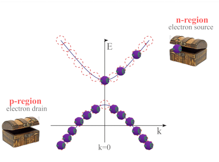
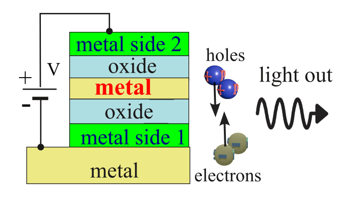
(conventional semiconductor LED): In a semiconductor LED, the device is typically composed of p-type and n-type regions. When a voltage is applied, holes and electrons are injected into the same region, where they combine and emit photons as the laser output.
(all-metal LED): Two metals are separated by an oxide layer. When a voltage is applied, electrons and holes tunnel through the oxide between metal layers and recombine, producing photons as the laser output, potentially allowing for an all-metal LED.
LED made of only metals |
|||||||||
|
|||||||||
click on image to enlarge it. Zayets 2024 |
![]() Can an LED be made entirely from metals?
Can an LED be made entirely from metals?
A. In principle, a similar approach as in a semiconductor LED could be applied for an all- metal LED. The electrons and holes constantly combine inside metal in great numbers. When two metals are separated by an oxide layer, electrons and holes tunnel through the oxide between metal layers and recombine, producing photons, which could be potentially used as the laser output allowing for an all-metal LED.
LED band requirements |
|||||||||||||||
|
|||||||||||||||
click on image to enlarge it. Zayets 2024 |
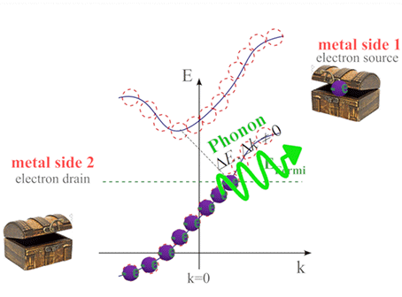
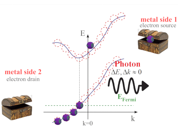
![]() Why does a direct-band semiconductor emit photons, while an indirect-band semiconductor emits phonons, but not photons?
Why does a direct-band semiconductor emit photons, while an indirect-band semiconductor emits phonons, but not photons?
A. This difference arises from the relationship between energy, momentum, and wave vector. For the same energy, a phonon has a much larger momentum and wave vector than a photon.
Momentum is inversely proportional to wave speed. The speed of sound (~300 m/s in air) is much slower than the speed of light (~3 × 10^8 m/s). Consequently, for a given energy, the momentum of a phonon is about a million times larger than that of a photon.

wher k is wave vector, ω is angular frequency and v is the speed of the wave particle.
In a direct-band semiconductor, the momentum (or wave vector) of an electron at the bottom of the conduction band is nearly the same as that of a hole at the top of the valence band. This means the transition between these states can be accompanied by a photon, which has a small momentum. Thus, photon emission is possible.
In an indirect-band semiconductor, however, the momentum of the electron at the bottom of the conduction band is very different from that of the hole at the top of the valence band. For a transition between these states, a wave particle with a much larger momentum, such as a phonon, is required to conserve momentum. As a result, the emission of photons is not possible, and phonon-assisted processes dominate.
| Video 2. |
|---|
| video 2 explores possibilities to fabricate Laser Emitting Diode (LED). Importance of the required precise engineering of band structure and Fermi level within metals and tackling the issue of strong light absorption in metals |
![]() Why does photon emission only occur for electron transitions from the top of the conduction band to the bottom of the valence band? Why can't the transition happen from a state in the middle of the conduction band or to a state in the middle of the valence band, where there is momentum matching for an indirect semiconductor??
Why does photon emission only occur for electron transitions from the top of the conduction band to the bottom of the valence band? Why can't the transition happen from a state in the middle of the conduction band or to a state in the middle of the valence band, where there is momentum matching for an indirect semiconductor??
A. The time an electron spends in a state in the middle of the conduction band is very short, far too brief for an electron transition to the valence band and photon emission to occur. For a photon to be emitted, the electron must remain in a quantum state long enough to allow the transition to the valence band, and this requires two conditions:
![]() (condition 1): Electron Accumulation:
(condition 1): Electron Accumulation:
A sufficient number of electrons need to accumulate in the conduction band, leading to population inversion—where the number of electrons in a state of the conduction band exceeds those in a state of the valence band. This is essential for stimulated emission and photon generation.
![]() (condition 2): Transition Time:
(condition 2): Transition Time:
The electron transition from the conduction band to the valence band takes a finite amount of time, approximately equal to a quarter of the Rabi oscillation period. During this time, the electron must remain in its quantum state without being scattered.
A similar scenario applies to the valence band. States in the middle of the valence band remain unoccupied only for very short periods, making them unsuitable for electron transitions that result in photon emission. Thus, photon emission occurs only when electron transitions occur from the top of the conduction band to the bottom of the valence band.
![]() Why are electron transitions within a band very fast, while transitions between bands are much slower?
Why are electron transitions within a band very fast, while transitions between bands are much slower?
A. Intra-band transitions (within a single band) are rapid because there are many closely spaced quantum states with small differences in energy and momentum. Frequent electron scattering events (e.g., due to phonons, impurities, or other electrons) easily move the electron toward the lowest available energy state. These transitions occur quickly as they do not require significant changes in momentum or energy, and conservation laws are easily satisfied.
Inter-band transitions (between different bands), on the other hand, take much longer due to two key reasons:
![]() (reason 1): Large energy and momentum differences:
(reason 1): Large energy and momentum differences:
States in different bands typically have significant differences in both energy and momentum. Standard scattering processes cannot facilitate these transitions, as they would violate the conservation of energy and momentum. For an electron to transition between bands, an additional particle (such as a photon or phonon) is needed to balance the energy and momentum difference, which makes these transitions less frequent and slower.
![]() (reason 2): Different spatial symmetries:
(reason 2): Different spatial symmetries:
Transitions between states with different symmetries are less probable because the overlap of their wavefunctions is smaller. As a result, these transitions take longer due to the lower probability of such interactions.
Together, these factors make inter-band transitions significantly slower than intra-band transitions.
 challenge with all-metal LED design
In semiconductor-based LEDs, the operation is not solely based on the different charges of electrons and holes but on differences in their spatial symmetry. Electrons in the conduction band typically have s-symmetry, while holes in the valence band have p-symmetry. This difference in symmetry reduces the probability of electron-hole interaction, allowing enough time for them to recombine radiatively and produce photons, while minimizing non-radiative recombination.
In contrast, in metals, both electrons and holes share the same symmetry, leading to very fast, non-radiative recombination. As a result, they combine too quickly to produce photons, making it difficult to generate light through radiative recombination.
![]() (fact): Stimulated emission of light occurs only when the population of electrons in a higher energy state exceeds that of the lower energy state (population inversion).
(fact): Stimulated emission of light occurs only when the population of electrons in a higher energy state exceeds that of the lower energy state (population inversion).
In semiconductors, electrons and holes have different spatial symmetries, which slows their non-radiative recombination, helping to maintain a higher population of the upper energy level.
In contrast, in metals, electrons and holes share the same spatial symmetry, leading to rapid recombination. This quick recombination reduces the population of the higher energy state below that of the lower energy state, preventing the necessary population inversion for laser emission.

![]() (solution 1): Utilize a specific metal that has two energy bands with distinct symmetries at its Fermi level.
(solution 1): Utilize a specific metal that has two energy bands with distinct symmetries at its Fermi level.
In this case, electrons will tunnel into the higher energy band and remain there for a relatively long time before relaxing into the lower energy band. The difference in spatial symmetries between the two bands slows down the recombination process, allowing for a sustained population of electrons at the higher energy level. This prolonged population could enhance the efficiency of photon emission by reducing non-radiative recombination.
![]() (solution 2): Increase of the tunneling time
(solution 2): Increase of the tunneling time
If hole-electron recombination occurs during tunneling, increasing the tunneling time can extend the duration that electrons remain in the higher energy state. This extended lifetime enhances the population of electrons at the higher energy level, potentially improving the efficiency of photon emission.
LED made only from metals |
||||||||||||
 |
||||||||||||
|
||||||||||||
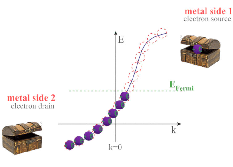
| When a voltage is applied across three metal regions, the electron energy becomes higher in the metal on side 1 and lower in the metal on side 2. As a result,high-energy electrons are injected from the metal on side 1, while low- energy holes are injected from the metal on side 2. Due to very fast electron scattering within the bands, the high-energy electrons rapidly move down, and the low-energy holes quickly move up. | ||||||||||||
| click on image to enlarge it. Zayets 2024 |
When discussing an "all-metal LED," one significant challenge that arises is the strong light absorption inherent to metals. Metals are well-known as some of the strongest absorbers of light. This raises a critical question:What is the benefit of generating laser light inside a metal if that light is immediately absorbed? At first glance, it might seem illogical to fabricate an all-metal LED if the emitted light cannot effectively escape the metal.
A. The all-metal LED can be optimized to ensure that the emitted light is minimally (nearly not) absorbed by the metal.
![]() (fact): There are many optical devices made of a metal and still having a low optical absorption.
(fact): There are many optical devices made of a metal and still having a low optical absorption.
![]() (Example 1): conventional mirror. Even though the reflective coatings in mirrors are made from metals like aluminum or silver, the mirror absorbs nearly no light and reflects nearly all of it.
(Example 1): conventional mirror. Even though the reflective coatings in mirrors are made from metals like aluminum or silver, the mirror absorbs nearly no light and reflects nearly all of it.
![]() (Example 2): plasmonic optical devices. In plasmonic devices, the overall loss due to light absorption is much smaller than you might expect. In fact, with proper design, the losses in a plasmonic device can be comparable to those in conventional, metal-free optical devices. Please see the technology of low-loss plasmonic devices, which I have developed for Si Photonics here.
(Example 2): plasmonic optical devices. In plasmonic devices, the overall loss due to light absorption is much smaller than you might expect. In fact, with proper design, the losses in a plasmonic device can be comparable to those in conventional, metal-free optical devices. Please see the technology of low-loss plasmonic devices, which I have developed for Si Photonics here.
![]() (strategy 1): Surface Plasmons
(strategy 1): Surface Plasmons
Unlike conventional light waves that propagate through the bulk of a material, surface plasmons are confined to the surface of a metal. As a result, the electromagnetic field of the plasmon resides mostly in the adjacent dielectric material, with only a small fraction penetrating into the metal.. This limited penetration significantly reduces the absorption within the metal, thereby minimizing plasmonic losses.
![]() (strategy 2): Blocking free-electron absorption
(strategy 2): Blocking free-electron absorption
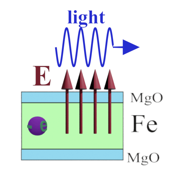
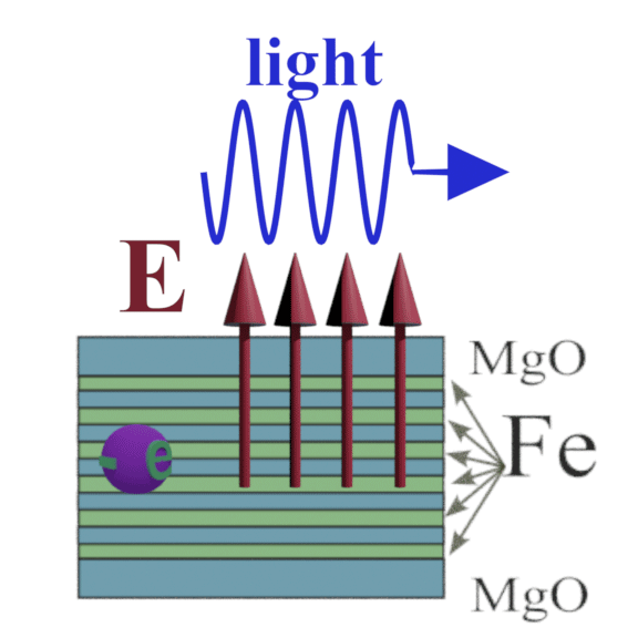
The free-electron absorption, which is the primary source of light loss in metals. This type of absorption occurs when the conduction electrons oscillate in response to the electric field of light. By designing structures composed of ultrathin metal layers—each less than 1 nanometer thick—separated by dielectric materials, electron movement perpendicular to the plane of the layers is effectively restricted. This configuration significantly suppresses free-electron absorption when light propagates along the structure and the electric field is oriented perpendicular to the plane.
Blocking free-electron absorption
Mechanism to block light absorption by a metal |
|||||||||||||||
|---|---|---|---|---|---|---|---|---|---|---|---|---|---|---|---|
| By employing these techniques, the light absorption in metals can be effectively reduced | |||||||||||||||
|
|||||||||||||||
| The oscillating electrical field (brown arrow) of TM- polarized light (blue arrow) forces a conduction electron (blue ball) to move perpendicularly to the interface. | |||||||||||||||
| click on image to enlarge it. | |||||||||||||||
| Zayets 2024.12 |
![]() (note) This same mechanism is utilized in the fabrication of thin-film light polarizers.
(note) This same mechanism is utilized in the fabrication of thin-film light polarizers.
Answer: The required thickness depends on the electron mean free path of the material. To block free-electron absorption, the metal layer thickness must be at least smaller than the electron mean free path.
In semiconductors, where the electron mean free path is relatively long, electron confinement occurs at a layer thickness of about 10–15 nm.
In metals, however, the electron mean free path is much shorter, so the metal layer must be extremely thin—typically less than 1 nm, with a typical range of about 0.4–0.6 nm.
(conventional semiconductor FET): In a semiconductor-based FET, two n-type regions are separated by a p-type region. Without a gate voltage, no current flows between the source and drain because the p-n junction is reverse-biased. When a gate voltage is applied, the Fermi level in the p-type region shifts, converting a small area under the gate from p-type to n-type, which opens the channel and allows current to flow.
(all-metal FET): There is no feasible design
![]() Why is it not feasible to make a Field-Effect Transistor (FET) of only metals without usage of a semiconductor?
Why is it not feasible to make a Field-Effect Transistor (FET) of only metals without usage of a semiconductor?
A. The essential principle behind the operation of an FET is the ability of the semiconductor to switch between a conductive and non-conductive state.
However, it is not feasible to create an FET using only metals. Metals are always conductive, and even though applying a gate voltage can shift the Fermi level, the metal will remain highly conductive. As a result, the required switching mechanism between conductive and non-conductive states cannot be achieved solely with metals.
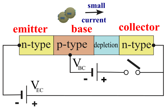
(conventional semiconductor Bipolar Transistor): In a semiconductor-based bipolar transistor, two n-type regions are separated by a very thin p-type region. This thin p-region allows electrons to diffuse between the two n-type regions. The voltage applied between the p-type region and one of the n-regions modulates the depletion width, effectively changing the width of the p-region. This, in turn, alters the diffusion time of the electrons through the p-region, thereby modulating their transmission and controlling the emitter-collector current.
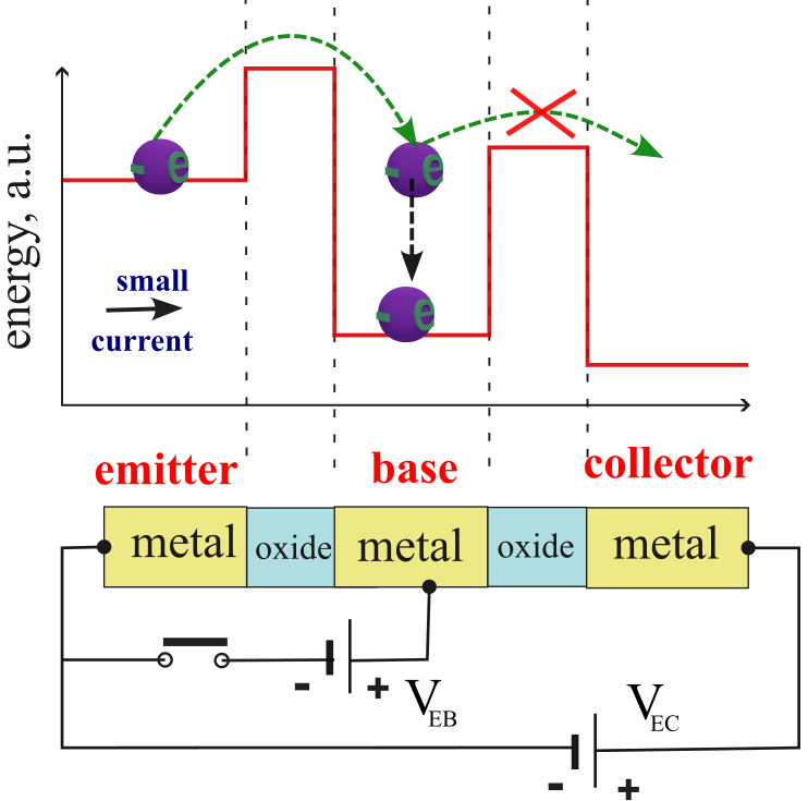
(all-metal Bipolar Transistor): In the design of an all-metal bipolar transistor design the three metals would serve as the emitter, base, and collector, with oxide layers inserted between each region to act as tunnel barriers. The current from emitter to collector flows via tunneling, and the base voltage modifies the height of the tunnel barrier, thereby modulating the emitter-collector current.
Bipolar Transistor made of only metals |
|||||||||
|
|||||||||
click on image to enlarge it. Zayets 2024 |
challenge with this all-metal Bipolar Transistor design.One key feature of semiconductor-based transistors is the relatively long interaction time between electrons and holes. This extended interaction allows electrons to travel significant distances within the p-type region, meaning even a small change in the effective thickness of the p-region can greatly influence electron transmission.
For this reason, creating a highly efficient bipolar transistor using only metals is quite challenging.
(device 2): Field-Effect Transistor (FET) made of only metals
(device 3): Bipolar Transistor made of only metals
() challenge with this all-metal Bipolar Transistor design
() Operation of semiconductor bipolar transistor
() Operation of all- metal bipolar transistor
Operation of all- metal bipolar transistor |
|||||||||
|---|---|---|---|---|---|---|---|---|---|
|
|||||||||
| Zayets 2024, click on image to enlarge it |
This approach explores novel concepts and mechanisms that have not been utilized in semiconductor-based devices. These new principles would be specifically designed to leverage the unique properties of metals, potentially leading to innovative types of electronic and data-processing devices that operate in fundamentally different ways from their semiconductor counterparts. One such unique property of metals is ferromagnetism, along with the associated phenomenon of magnetoresistance.
Ferromagnetic metals exhibit spontaneous magnetic ordering, which can be harnessed to create devices that rely on the manipulation of magnetic domains rather than traditional charge-based mechanisms. Additionally, magnetoresistance—where the electrical resistance of a material changes with respect to the magnetization direction- may be used as a current switching mechanism. These properties could be key in developing all-metal devices that outperform or complement existing semiconductor technologies.
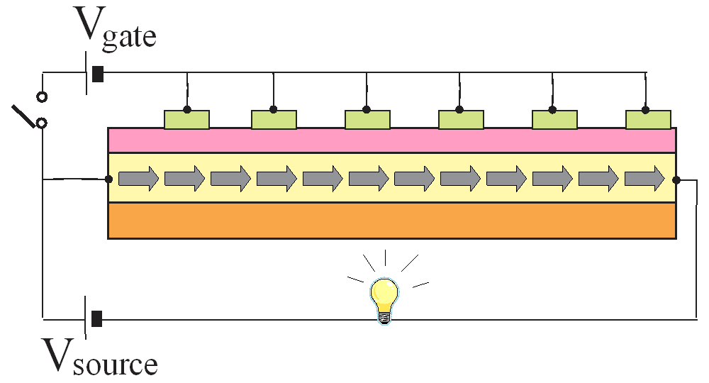
Design 1 of proposed all-metal transistor. |
||||
|
||||
Ferromagnetic metal with in-plane equilibrium magnetization. click on image to enlarge it |
Design 1. Ferromagnetic metal with in-plane equilibrium magnetization
gate voltage: DC or pulse
The magnetization direction under the gate is changed by the VCMA effect.
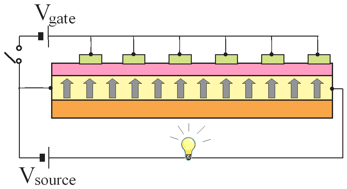
Design 2. Ferromagnetic metal with perpendicular -to -plane equilibrium magnetization
Design 2 of proposed all-metal transistor. |
||||
|
||||
Ferromagnetic metal with in-plane equilibrium magnetization. click on image to enlarge it |
gate voltage: pulse only
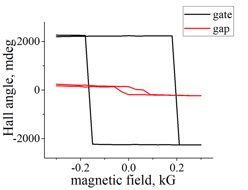
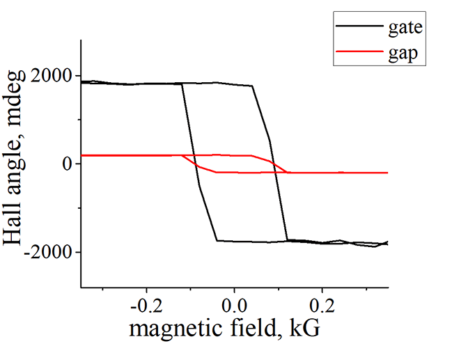
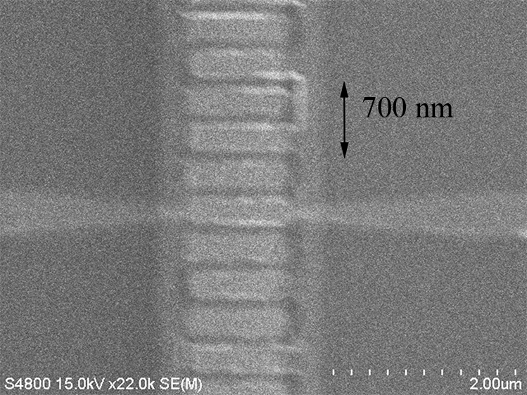
High MR in FeBTb nanowire with periodically Pt electrode |
|||||||||
|
|||||||||
Detailed experimental data see below. click on image to enlarge it |
Pt induces perpendicular magnetic anisotropy (PMA) in FeBTb.
Additionally, there is a volume-type PMA in FeBTb. As a result, a thicker FeBTb nanowire has a larger PMA than a thinner nanowire.
Under Pt gate the PMA is larger than in the gap between electrodes, because interface PMA at Pt/FeBTb interface and because in this region the FeBTb is thicker.
|
||||||
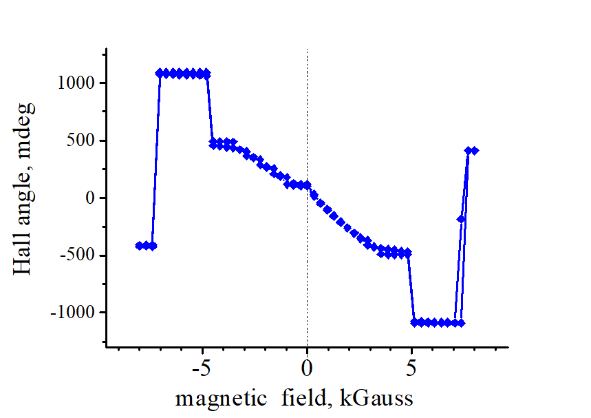
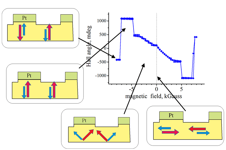
| (left) FeBTb nanowire with Pt periodical gate is directed from bottom to top. The Hall probe is directed from left to right. For this measurement the hall angle represents the average Hall angle in region under gate and in the gap between gate electrodes. magnetic field is applied perpendicularly to the sample. Measurement date: July 2015. click on image to enlarge it |
FeBTb is a compensated ferromagnetic. Magnetic moments of Fe and Tb are coupled antiferromagnetically.
the FeBTb with small Tb concentrations was studied. As a result, the total magnetization of Fe is larger than the magnetization of Tb atoms
The PMA in the FeBTb film is the volume-type. The PMA in the FeBTb film increases when thickness increases. The equilibrium magnetization of used FeBTb (3 nm) is in-plane.
no magnetic field: H=0 kG
Magnetization is in-plane. The magnetization of Fe and Tb are anti parallel each other. Magnetization of Fe in regions under gate and between gates are anti parallel each other as well.
magnetic field: from 0 to 5 kG
Both the magnetic moments of Tb and Fe turn toward the magnetic field. The angle between the magnetic moments becomes smaller than 180 degrees.
magnetic field: from 5 to 7.5 kG
|
||
Red arrow shows suggested magnetization of Fe. Blue arrow shows suggested magnetization of Tb. click on image to enlarge it |
Anti ferromagnetic interaction between Fe and Tb becomes stronger than the dipole interaction with external magnetic field. The magnetic moments of Tb and Fe turn to be anti parallel each other again. In both regions under and between gate the magnetic moments of Fe become parallel.
magnetic field: above 7.5 kG
The magnetic moments of Fe become anti parallel in regions under Pt gate and between gates.
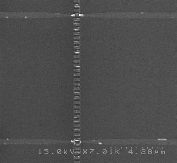
|
||||||||||||
Top SEM view. click on image to enlarge it |
In order to optimize the transistor, it is important to measure the magnetization independently and simultaneously in regions under the electrode and in gap between electrodes. It clarifies whether
(1) magnetization is magnetically decoupled in these regions
(2) magnetization direction in each region
The exchange interaction between regions under gate and in gap between gates forces forces
Decoupling of magnetization in regions under gate and in gap between gates |
|||||||||
|
|||||||||
click on image to enlarge it |
Gate with periodical change of polarity |
||
In this structure, a gate voltage of opposite polarities is applied to neighbor gate electrode. The Hall probe (from left and from right) is precisely aligned to measure the magnetization direction at each gate electrode. Top SEM view. click on image to enlarge it |
In this structure, a gate voltage of opposite polarities is applied to neighbor gate electrode. As a result, under one gate electrode the PMA of the nanowire increases and under neighbor electrode the PMA decreases. That enhances the formation the gate-voltage-induced domain structure in the nanowire.
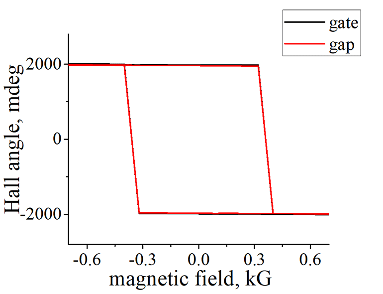
Pinning of domain wall & magnetization in gap between Pt gate electrodes |
FeBTb nanowire with Pt periodic electrode. | FeBTb nanowire with Pt periodic electrode. |
 |
 |
|
Basic structure of all-metal transistor. (1)ferromagnetic nanowire; (2) gate oxide (3) gate electrode (4) material to enhance interfacial PMA in the gap; (5) substrate. click on image to enlarge it |
Periodic Pt electrodes on a ferromagnetic nanowire, which induces the periodical PMA in the wire. The front Hall probe contacts the region under the Pt electrode. The back Hall probe contacts the region in the gap between Pt electrode. The region in the gap is deeply etched into the nanowire in order to pin a domain wall at boundary between these regions. click on image to enlarge it | The same as left picture, but SiO2 layer is not shown. click on image to enlarge it |
The pinning of domain wall and pinning of magnetization in gap between gate electrodes are critically important for the operation of the transistor.
A different thickness of nanowire is used to pin firmly the domain at the boundary between the gate electrode and the gap.
The material with a large interfacial PMA is deposited in the gap between gate electrode in order to pin the magnetization in this region
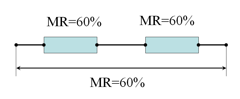
 Effect of accumulated magneto-resistance
In fact, the magneto-resistance (MR) is not accumulated effect. The total magneto-resistance of two or more MR elements, which are connected either parallel or in series, is smaller or equal to the magneto-resistance of each MR element.
![]() In contrast, in a nanowire with magnetic domains the magneto-resistance may be accumulated
In contrast, in a nanowire with magnetic domains the magneto-resistance may be accumulated
|
||||
|
||||
In either case, the total MR equals to the MR of each element! click on image to enlarge it |
Example 1: Two MR elements are connected in series
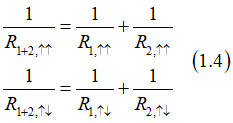
In this case total resistance can be calculated as
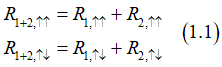
where ![]() are resistance of 1st and 2d elements of their two electrodes are parallel.
are resistance of 1st and 2d elements of their two electrodes are parallel. ![]() are resistance of 1st and 2d elements of their two electrodes are anti parallel.
are resistance of 1st and 2d elements of their two electrodes are anti parallel.
The total magneto-resistance can be calculated as
in the case when two MR elements have an equal magneto-resistance ![]() , the total MR is the same as MR of each element
, the total MR is the same as MR of each element
![]()
Example 2: Two MR elements are connected in parallel
In this case total resistance can be calculated as
in the case when MR and resistance are equal
The total resistance can be calculated from Eq.(1.4) as

From Eq. (1.6), the total MR is calculated as

![]() the total MR is the same as MR of each element
the total MR is the same as MR of each element
![]()
|
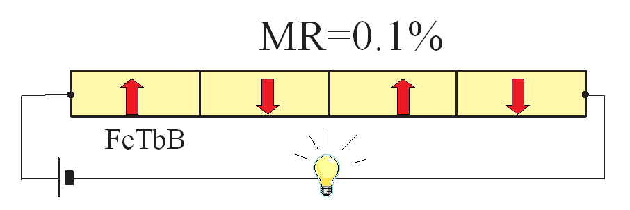
||||||||||||
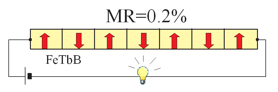
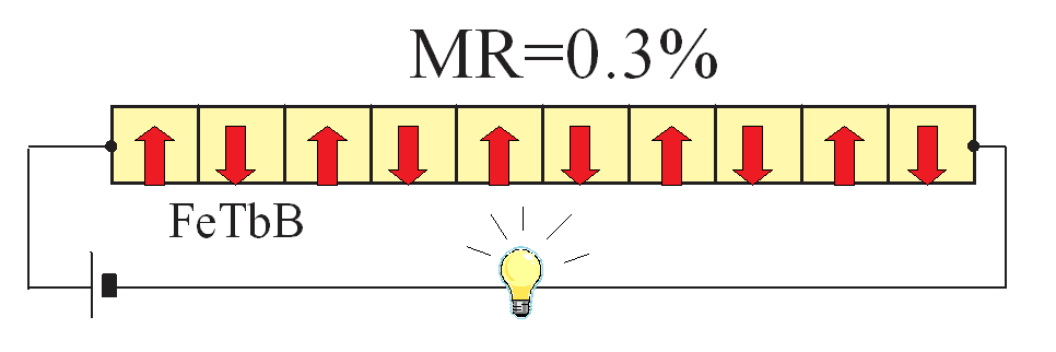
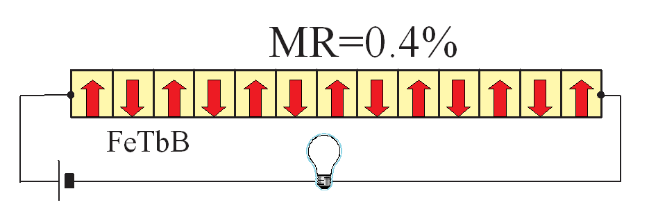
MR increases when number of domain walls increases and domain size decreases!! |
||||||||||||
| Click on image to enlarge it |
The magneto-resistance of a ferromagnetic nanowire with domain walls is calculated as
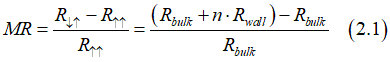
where Rbulk is the bulk resistance of the nanowire without any domains, Rwall is the resistance of one domain wall and n is number of domain walls.
From Eq(2.1), is MR is calculated as

The magneto-resistance (MR)increases when number of domain walls n increases and domain size decreases!!
 How large is the resistance Rwall of one domain wall?
1. The smaller domain size , the larger MR !! 2. The shorter domain wall,.the large MR!! |
|
Click on image to enlarge it |
The change of resistance on nanowire, which is made of Fe or Co, is about 0.1-0.01% (70 K) ( Kent et al, JCMCP (2001)) . Usually, it is about the same magnitude as the resistivity change due to the Anisotropic magnetoresistance (AMR). I have never observed the domain wall resistance in Fe, FeB, Co in my experiments at room temperature. Even though I have fabricated a nanowire made of these materials with 50 nm long domains, which was checked by Hall measurements (See here). In contrast, a nanowire made of a compensated ferromagnet (like FeBTb) always shows a substantial domain wall resistance and a substantial AMR. I am not sure weather the domain wall resistance and the AMR are related.
The resistance of one domain was measured in 60-nm-wide FePd nanowire at 17 K. It was about 0.01 Ohm, when total resistance of nanowire was 3 Ohm (Danneau et al, PRL 2002)
![]() method 1: Reduce size of a domain
method 1: Reduce size of a domain
The smaller domain size , the larger MR ! See fig. above. The periodically-modulated PMA is the method to obtain the shortest domain.
![]() method 2: Make a shorter domain wall
method 2: Make a shorter domain wall
The magnetization direction is opposite for neighbor domains. The spin direction of spin-polarized conduction electrons is along the magnetization in the bulk of the domain. However, in the region of the domain wall the spin-polarization becomes zero (See here). The magneto-resistance may occurs when electron current is passing through the regions of different spin polarization of the conduction electrons. The steeper the change of spin polarization is, the larger the MR is. Therefore, the domain structure with the shortest domain wall is required in order to obtain a substantial MR.
Example: (1) in Fe:MgO:Fe MTJ device, the spin polarization of the conduction electrons changes sharply from one Fe electrode to another Fe electrode. As a result, the MR is very high ~100 %; (2) in Co:Cu:Co p-GMR device , the spin polarization changes very gradually from one Co electrode to another Co electrode. As a result, the MR is moderate ~0.1 %; It should be noted that other material parameters influence the MR, but tendency is clear.
![]() method 3. Use a compensated ferromagnetic material or an antiferromagnetic material as a material of nanowire
method 3. Use a compensated ferromagnetic material or an antiferromagnetic material as a material of nanowire
Up to now (Aug.2018) I have never detected any domain wall resistance in a nanowire made of FeB or Co or Fe, which were measured at room temperature. However, I often detect the domain wall resistance in the compensated ferromagnetic FeBTb.
![]() method 4 Use a material with a low conductivity. Use a "bad" conductor
method 4 Use a material with a low conductivity. Use a "bad" conductor
All spin-dependent features more manifest themselves in a metal with a lower conductivity (in a "bad" conductor). The reason for this is that the nature of electrical current is very different from that in a "good" conductor. (See here). The magneto-resistance only may occur in the "bad" conductor, but it can not be any magneto-resistance in the "good" conductor (See here).
![]() Why the most of reports on the resistance of a domain wall is done at low temperature?
Why the most of reports on the resistance of a domain wall is done at low temperature?
There are two reasons for that:
reason 1: The spin polarization of the conduction electrons becomes larger due reduction of the spin relaxation time (See here).
reason 2: The gradient of the spin polarization in the region of the domain wall becomes sharper.
![]() Main challenge is to obtain a sufficient domain wall resistance.
Main challenge is to obtain a sufficient domain wall resistance.
It can be only achieved in a metal with a high resistivity. There is a fundamental reason for that (See here)
Many neuromorphic specific circuits can be represented as neural gates performing the operation of a “dot product” of vectors of analog inputs and stored weights (synapses), followed by a non-linear threshold function (a neuron).
A logic element has only two states: 0 and 1. For neuron computing, a memory element with a larger number of states is required. In the proposed design, the resistance of the device can be increased by given amount when the gate voltage is applied only to some (not to all) electrodes and only some of domains are reversed.

My Videos explaining features and challenges for design and fabrication of a transistor made entirely from metals |
|||||||||
|---|---|---|---|---|---|---|---|---|---|
|
|||||||||
| click on it to play or open in YouTube |
![]()
![]() I am strongly against a fake and "highlight" research
I am strongly against a fake and "highlight" research ![]()
![]()
![]()
![]()
![]()
![]()
I will try to answer your questions as soon as possible