Dr. Vadym Zayets
v.zayets(at)gmail.com
My Research and Inventions
click here to see all content |

Dr. Vadym Zayetsv.zayets(at)gmail.com |
|
|
more Chapters on this topic:IntroductionTransport Eqs.Spin Proximity/ Spin InjectionSpin DetectionBoltzmann Eqs.Band currentScattering currentMean-free pathCurrent near InterfaceOrdinary Hall effectAnomalous Hall effect, AMR effectSpin-Orbit interactionSpin Hall effectNon-local Spin DetectionLandau -Lifshitz equationExchange interactionsp-d exchange interactionCoercive fieldPerpendicular magnetic anisotropy (PMA)Voltage- controlled magnetism (VCMA effect)All-metal transistorSpin-orbit torque (SO torque)What is a hole?spin polarizationCharge accumulationMgO-based MTJMagneto-opticsSpin vs Orbital momentWhat is the Spin?model comparisonQuestions & AnswersEB nanotechnologyReticle 11
more Chapters on this topic:IntroductionTransport Eqs.Spin Proximity/ Spin InjectionSpin DetectionBoltzmann Eqs.Band currentScattering currentMean-free pathCurrent near InterfaceOrdinary Hall effectAnomalous Hall effect, AMR effectSpin-Orbit interactionSpin Hall effectNon-local Spin DetectionLandau -Lifshitz equationExchange interactionsp-d exchange interactionCoercive fieldPerpendicular magnetic anisotropy (PMA)Voltage- controlled magnetism (VCMA effect)All-metal transistorSpin-orbit torque (SO torque)What is a hole?spin polarizationCharge accumulationMgO-based MTJMagneto-opticsSpin vs Orbital momentWhat is the Spin?model comparisonQuestions & AnswersEB nanotechnologyReticle 11
|
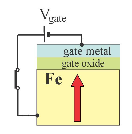
Voltage-controlled magnetism. The VCMA effect Spin and Charge TransportAbstract:The voltage-controlled magnetic anisotropy (VCMA) effect describes the fact that in a capacitor, in which one of electrodes is made of a thin ferromagnetic metal, the magnetic properties of the ferromagnetic metal changes, when a voltage is applied to the capacitor.Magnetic parameters, which depend on the gate voltage:
|
What is the VCMA effect? |
||||||||
| The VCMA effect describes the modulation of the magnetic properties of ferromagnetic metal by a gate voltage | ||||||||
|
||||||||
| click on image to enlarge it |
Applications of the effect:
1) Voltage-switched magnetic random access memory (MRAM)
Under an applied voltage the magnetization direction of the ferromagnetic metal may be changed or even reversed. This magnetization-switching mechanism can be used as a data recording method. When an electrical pulse reverses magnetization direction, the data is memorized in the ferromagnetic metal by means of its two opposite magnetization directions. Such a recording mechanism is fast and energy-efficient. It may be used in magnetic the random access memory (MRAM) and the all-metal transistor.
![]() As Nov. 2018, the physical origin of the VCMA effect is still unclear. Many experimental and theoretical research are still going in order to clarify it.
As Nov. 2018, the physical origin of the VCMA effect is still unclear. Many experimental and theoretical research are still going in order to clarify it.
Based on the Modulation of Fermi level
![]() Problem: Estimated change of the Fermi level is small. It is only 4.5 eV per 1 V of gate voltage (see below)
Problem: Estimated change of the Fermi level is small. It is only 4.5 eV per 1 V of gate voltage (see below)
![]() Origin 1
Origin 1
![]() Origin 2
Origin 2
Possible origins of VCMA effect |
||||||||||||||||
|---|---|---|---|---|---|---|---|---|---|---|---|---|---|---|---|---|
|
||||||||||||||||
| As Feb. 2019, the origin of the VCMA effect is still unclear | ||||||||||||||||
| click on image to enlarge it |
Not related to modulation of Fermi level
![]() Origin 3
Origin 3
![]() Origin 4
Origin 4
![]() Origin 5
Origin 5
Undesired effects
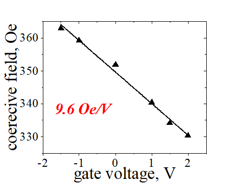
I use 5 independent measurements of the VCMA effect. All measurements have similar tendency of the linear dependence on gate voltage and the negative polarity of the dependence.
Measurements 1
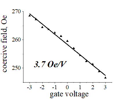
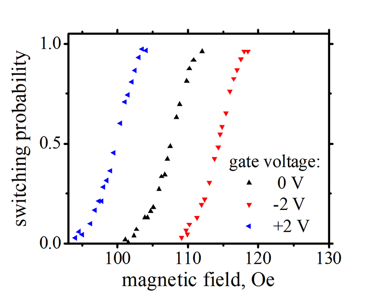
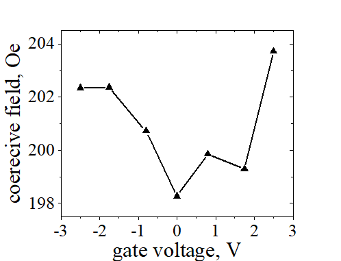
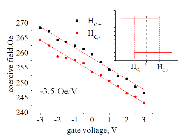
measurement 1: Voltage-dependence of coercive field |
||||||
|
||||||
FeB sample. click on image to enlarge it. |
slope: negative; gate-voltage polarity change: changes sign
For measurements, this method is used. It is very sensitive technique. It allows to detect a very tiny changes of the PMA under a gate voltage. The coercive field increases under a negative gate voltage and it decreases under a positive gate voltage. Most of samples show a perfect linear dependance.
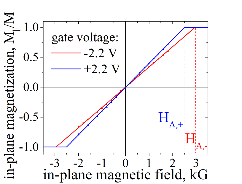
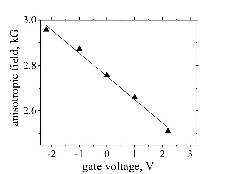
measurement 2: Voltage-dependence of anisotropy field |
||||||
|
||||||
Measurement date: May 2018. FeB nanomagnet. click on image to enlarge it. |
slope: negative; gate-voltage polarity change: changes sign
The anisotropy field is the the field, at which initially-perpendicular magnetization turns completely to the in-plane direction. The anisotropy field increases under a negative gate voltage and it decreases under a positive gate voltage. The anisotropy field is proportional to the PMA energy (For details see here)
slope: negative; gate-voltage polarity change: changes sign
For measurements, this method is used. It is very sensitive technique. It allows to detect a very small change of magnetic properties. This method allows to measure simultaneously the retention time and magnetization. Most of samples show substantial change of the retention time and Δ, In contrast, this method does not detect any modulation of the magnetization by the gate voltage.
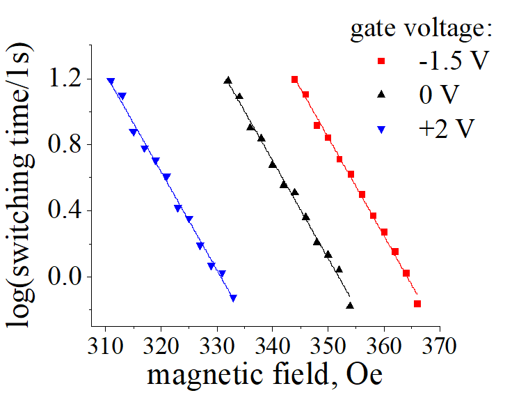
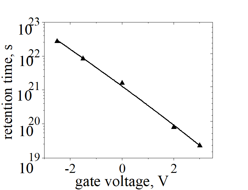
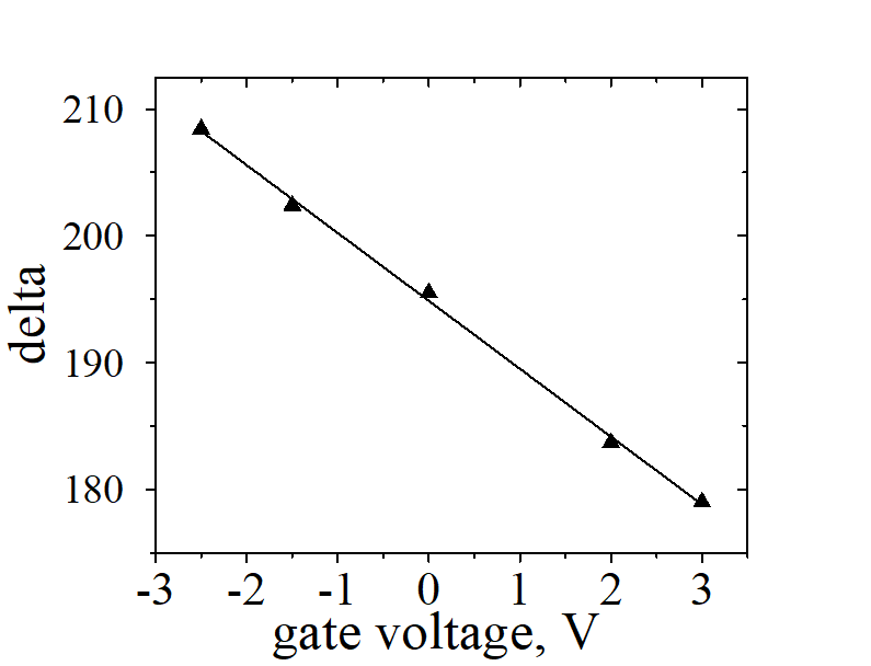
Figure 11 (left) shows the dependence of the switching time on the magnitude of an external perpendicular magnetic field. On a logarithmic scale, the switching time is linearly proportional to the magnetic field. Therefore, the magnetization switching is well described by the Arrhenius law (Details see here) even in the case when magnetic properties are changed by a gate voltage. The switching time becomes longer at a negative gate voltage and shorter at a positive gate voltage. From this Eq, the slope of the lines is proportional to Meff and the horizontal offset is proportional to retention time and consequently to EPMA. Figure 11 (center) shows the measured dependence of the retention time on the gate voltage. On a logarithmic scale, the dependence is linear. The retention time increases at a negative gate voltage and decreases at a positive gate voltage. As can be seen from Fig. 11(left), the slope for each line is nearly the same. It means that the Meff is not significantly affected by the gate voltage. The Meff describes the average bulk magnetization during the magnetization reversal. It is not sensitive to a small change of magnetization in a thin region near the interface. Figure 11(right) shows the measured dependence of the Δ on the gate voltage. The dependence is linear. The Δ increases at a negative gate voltage and decreases at a positive gate voltage.
slope: negative; gate-voltage polarity change: changes sign
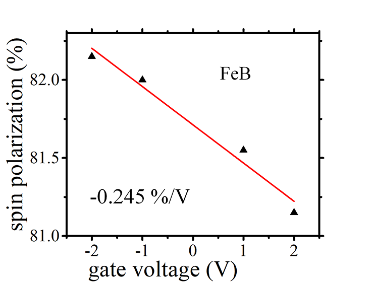
measurement 4: Voltage-dependence of spin polarization |
||||
|
||||
click on image to enlarge it |
The spin polarization (sp) in a ferromagnetic metal linearly increases under a negative gate voltage and linearly decreases under a positive gate voltage.
Measurements:
FeB (sp=81.7 %) : voltage-dependent change of sp=-0.245 %/V
FeCoB (sp=89.4 %) : voltage-dependent change of sp=-0.0068 %/V
A. The equilibrium spin polarization sp0 is larger in FeCoB sample than in FeB sample. As a result, the same change of the sp-d spin pumping causes a smaller change of sp0 in the FeCoB sample than in the FeB sample.
The spin polarization is different in a different ferromagnetic metal. The spin polarization is determined by a balance between the spin pumping and the spin damping. The spin pumping describes the conversion of spin-unpolarized electrons into the group of spin-polarized electrons. The spin damping describes the opposite conversion. (See details here). The origin of the spin pumping is the exchange interaction between conduction electrons and localized d-electrons (See here). The origin of the spin damping is scatterings on defects, the spin precession in an inhomogeneous magnetic field and so forth.
![]() Since the gate voltage modulates the spin polarization, either the spin pumping or the damping or both are modulated by the gate voltage.
Since the gate voltage modulates the spin polarization, either the spin pumping or the damping or both are modulated by the gate voltage.
A. Probably the gate voltage changes the spin pumping. However, the change of the spin damping is also possible.
Possible mechanism of the gate-voltage modulation of the spin polarization:
It can be assumed that a negative gate voltage enlarges the metal magnetization in a very thin region close to the gate interface. Due to the larger magnetization, the sp-d spin pumping should be enhanced. Such enhancement leads to a larger spin polarization.
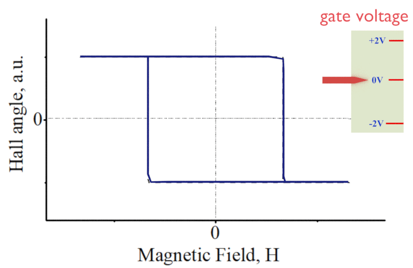
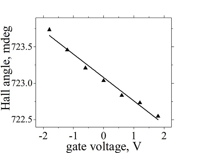
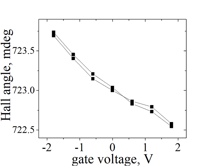
measurement 5: Voltage-dependence of Hall angle |
||||
|
||||
click on image to enlarge it |
slope: negative; gate-voltage polarity change: changes sign
The Hall angle increases under a negative gate voltage and it decreases under a positive gate voltage.
Figure 9 shows the gate-voltage dependency of the Hall angle in the FeB film. (See here details about Hall angle) All measurement points fit well in a straight line with a negative slope.
The Hall angle is proportional to the magnetization of the ferromagnetic metal, the spin polarization of the conduction electrons and the strength of spin-orbit interaction (See here).
 All measurements demonstrate the same tendency. The coercive field, anisotropy field, PMA energy, Hall rotation angle, and retention time decrease under a positive gate voltage and increase under a negative voltage.
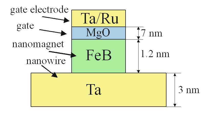
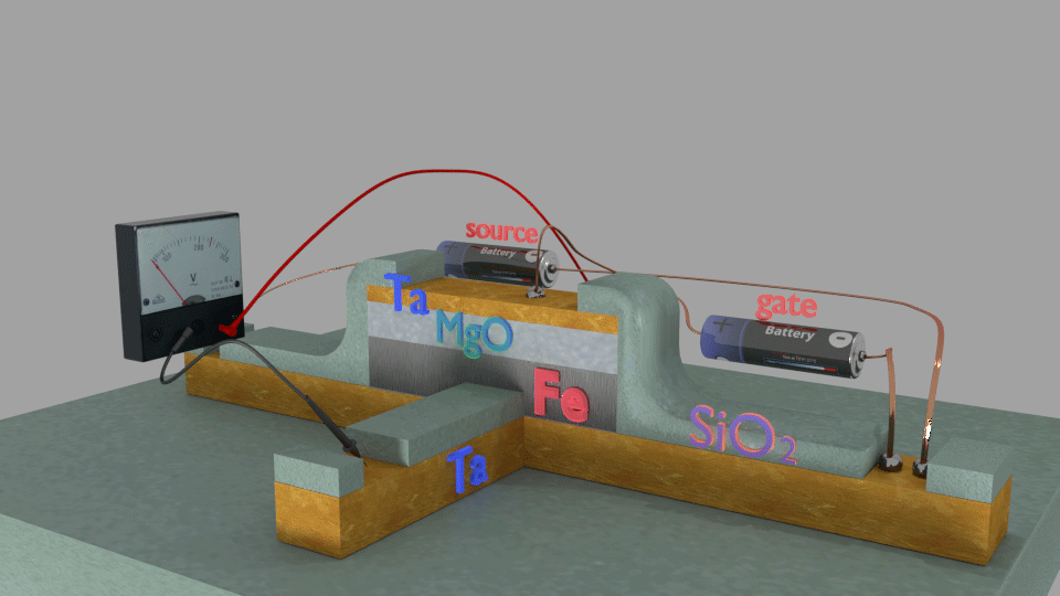
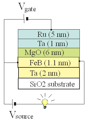
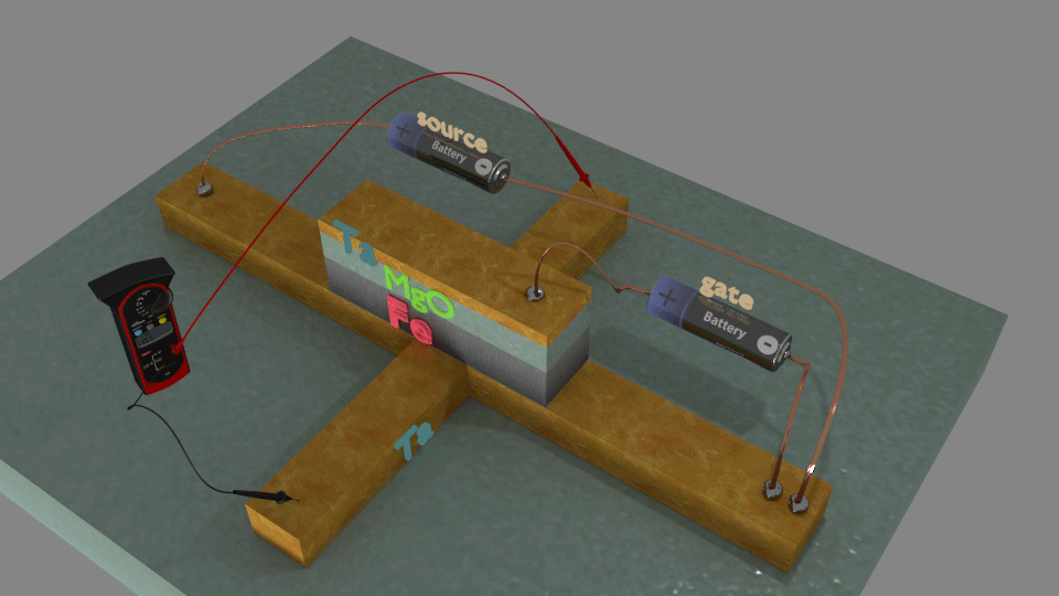
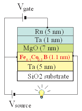
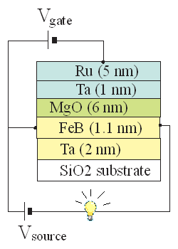
Samples for measurement of voltage- controlled magnetism |
||
|
||
Ta/FeB nanomagnet with MgO gate and Ta/Ru gate electrode. click on image to enlarge it. |
A thin nanowire of a ferromagnetic metal is used. A pair of Hall probe is used to extract magnetic properties of ferromagnetic nanowire. The source voltage is applied between two ends of the nanowire. The gate voltage was applied between one end of the nanowire and the gate electrode.
Yes, there is, but it does not exceed 0.1 uA. It depends on the area of the gate. Typically it is 0.01-0.001 uA at the maximum- used gate voltage. Such small current does not influence the measurement. The measurements of the tunneling current is important. Measurements of the tunneling current is important to estimate the density of deep defects in the MgO gate oxide ( See below)
It is the fabrication of the MgO gate oxide with the lowest density of the deep defects. I have developed an optimized growth method to reduce the density of the defect in the MgO gate oxide. However, some defect still remains and they influence the measured properties of the VCMA effect.
In the case of MgO gate oxide, two growth methods can be used
1. Conventional growth method of MgO gate (a lower quality & larger amount of defects)
EB evaporation of MgO at room temperature. MgO thickness: 7-10 nm
2. Optimized growth method of MgO gate (a higher quality & lower amount of defects)
At first, a 1 nm MgO was deposited at room temperature, next the sample was annealed at 2200 C for 30' and the remaining of the MgO gate oxide was grown at 2200 C. Three 30-minute growth interruptions after each 1 nm of growth were used to improve the MgO crystal quality. Total MgO thickness is 7-10 nm
This fabrication method of MgO gate increases the break-down voltage and to suppress the oxygen diffusion in the gate.
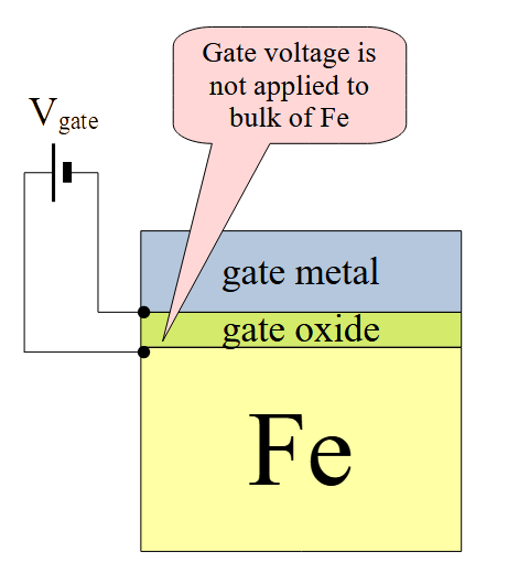
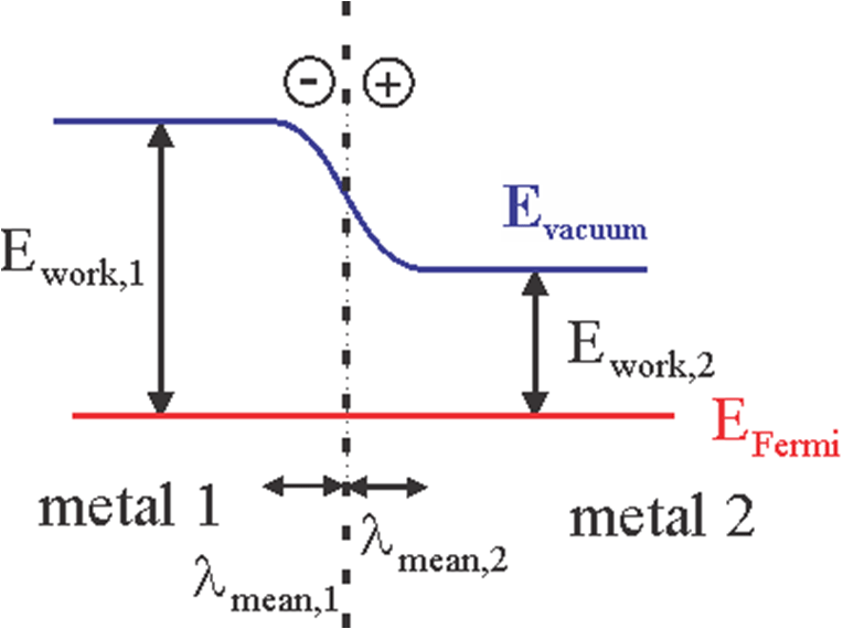
Inside a metal the electrical field is screened by free electrons and cannot penetrate deep inside the metal. As a result, the voltage, which is applied to the capacitor dielectric (gate), may penetrate into and affect only the few uppermost atomic layers of the metal near the gate. However, the change of magnetic properties of the uppermost layer by the gate voltage affects the magnetic properties of the whole film. This can be only the case if the interfacial perpendicular magnetic anisotropy (PMA) is affected by the gate voltage.
The interfacial PMA is the effect, which occurs due to a strong spin-orbit (SO) interaction in the upmost atomic layer of the metal[8]. As a result, the magnetic properties of only one upmost atomic layer strongly affect the magnetic properties of the whole film. Since the magnitude of the VCMA effect can be substantial, it is likely that the gate voltage affects the interfacial PMA. However, it is still unclear which particular properties of the upper layer or the whole film are changed by the gate voltage. The interfacial PMA depends on the magnetization of the film, atom arrangement and bonding at the interface. The gate-dependence of each of these properties may be the origin of the VCMA effect. The understanding of the details of the VCMA effect is important in order to optimize and possibly enhance the effect for a future practical application. In this paper we particularly emphasize our study on the symmetry and polarity the VCMA effect with respect to the reversal of the gate voltage. It might be a clue to clarify the origin of the VCMA effect.
PMA changes only in the case when
1. Magnetization is changed
2. Spatial symmetry of orbital is changed. (the orbital is deformed)
note: Only changes in uppermost layer affect the PMA.
The interface PMA occurs due to the strong spin-orbit (SO) interaction in the uppermost atoms of a metal at the gate. The SO interaction is a relativistic effect, which states that an electron experiences an effective magnetic field when it moves in a static electrical field. The SO effective magnetic field is proportional to 1/c2, therefore it is small. Only in a strong static electrical field, an electron may experience a substantial SO effective magnetic field. In a solid the electrical field is only strong enough in the close proximity of the nucleus in order to induce a substantial SO magnetic field of 1 kGauss or greater. However, in a central-symmetric electrical field of a nucleus the effective SO magnetic field is non-zero only when both the time-inverse symmetry and the spatial symmetry are broken. Otherwise, the effect cancels itself. The intrinsic magnetic field or the magnetization of a ferromagnetic metal breaks the time-inverse symmetry. As a result, the strength of the SO effective magnetic field and the value of the PMA energy are proportional to the magnetization. (For more details see here)
The second condition for the existing of the SO magnetic field is the breaking of the spatial symmetry. For example, an electron of the symmetry, which has the spherical orbital, does not experience any SO interaction, because the spatial symmetry is not broken for such orbital. An external electrical field can break the spatial symmetry. There are several possible orbital deformations, which may lead to the breaking of the spatial symmetry. Firstly, the external electrical field may deform the orbital along its applied direction. Secondly, the electrical field may shift the center of the orbital from center of the nucleus.
All experimental measurements of the gate-voltage dependence of different magnetic parameters have the similar tendency and they related to each other. They linearly decrease when the gate voltage increases and they linearly increase when the gate voltage decreases. A sample, in which the voltage dependence is stronger for one magnetic parameter, has a stronger voltage dependence of other magnetic parameters.
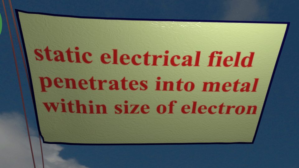
Static electrical field penetration into a metal |
|||||
|
|||||
Click on image to enlarge it. |
The electrical field is screened in a metal. That means the following. The conduction electron move in the electrical field and they are accumulated at boundary of the gate oxide until their own electrical field fully compensates the applied electrical field and the total electrical field becomes zero.
In contrast to a semiconductor, which can be depleted, a metal can not be depleted and the conduction electrons are accumulated in a thin region at non-conductive gate oxide. This region is very thin, but not infinitely thin. Its thickness is about the size of electron or the electron mean-free path λmean (for details, see here and here). Along the thickness of this region, the electrical field decreases towards zero.
The smaller the thickness of electron accumulation region is, the larger the VCMA becomes. (independently from the VCMA origin!).
The smaller the thickness of electron accumulation region is:
![]() the larger the density of electron accumulation becomes. As a result, the larger change of the Fermi level under a gate voltage becomes.
the larger the density of electron accumulation becomes. As a result, the larger change of the Fermi level under a gate voltage becomes.
![]() the larger the electrical field in this region becomes. As a result, the larger the orbital reconstruction becomes.
the larger the electrical field in this region becomes. As a result, the larger the orbital reconstruction becomes.
![]() the larger the stress and magnetostriction effect. It is because of a larger electrical field in this region and the electrical field is compress force.
the larger the stress and magnetostriction effect. It is because of a larger electrical field in this region and the electrical field is compress force.
![]() the stronger the oxygen electro diffusion becomes. It is because of a larger electrical field in this region, which induces the electro diffusion..
the stronger the oxygen electro diffusion becomes. It is because of a larger electrical field in this region, which induces the electro diffusion..
![]() The larger metal resistivity is, the larger the VCMA effect is (independently on the VCMA origin)
The larger metal resistivity is, the larger the VCMA effect is (independently on the VCMA origin)
Explanation: In a metal of a higher resistivity the mean free path of conduction electrons is shorter. As a result, the size of conduction electron is shorter, the penetration length of electrical field is shorter and therefore the VCMA is larger.
Note: AC electromagnetic field may also penetrates into a metal. This effect is called the skin effect. It has an electromagnetic origin, which is very different from the origin described above.
Origin 1: Change of magnetization under a gate voltage |
||||||
click on image to enlarge it |
![]() Supporting Facts:
Supporting Facts: ![]() The predicted polarity of VCMA is exactly the same as observed experimentally.
The predicted polarity of VCMA is exactly the same as observed experimentally. ![]() All experimental data point that the magnetization is change in a small region of metal close to the gate, which is predicted by this mechanism.
All experimental data point that the magnetization is change in a small region of metal close to the gate, which is predicted by this mechanism.![]() This mechanism predicts the dependence of the VCMA effect on the position of the Fermi level in the ferromagnetic metal. There some experimental hints that it is the case (See FeB/W multilayer below). Still such dependence need be clarify carefully.
This mechanism predicts the dependence of the VCMA effect on the position of the Fermi level in the ferromagnetic metal. There some experimental hints that it is the case (See FeB/W multilayer below). Still such dependence need be clarify carefully.
![]() Problems:
Problems: ![]() : Estimated change of the Fermi level is too small. It is only 4.5 eV per 1 V of gate voltage. In order to explain the experimental facts, it should be larger.
: Estimated change of the Fermi level is too small. It is only 4.5 eV per 1 V of gate voltage. In order to explain the experimental facts, it should be larger. ![]() This mechanism predicts the dependence of the VCMA effect depend on the material of the gate metal. Such dependence has not been observed experimentally yet. (I have checked W and Ta. I cannot find a substantial difference). A possible pinning of the Fermi level inside gate oxide make such experiment difficult.
This mechanism predicts the dependence of the VCMA effect depend on the material of the gate metal. Such dependence has not been observed experimentally yet. (I have checked W and Ta. I cannot find a substantial difference). A possible pinning of the Fermi level inside gate oxide make such experiment difficult.
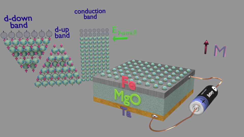
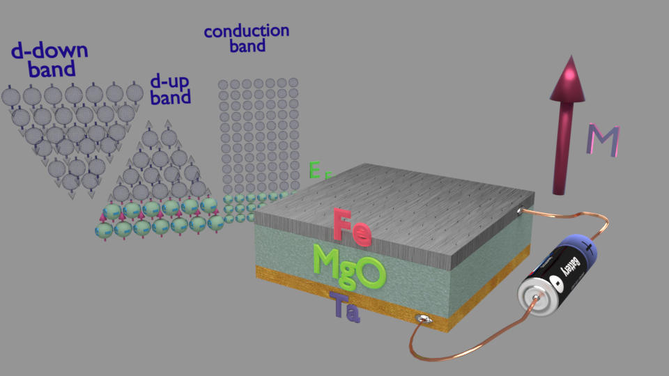
Under a gate voltage the conduction electrons are accumulated or depleted in the vicinity the gate oxide. It changes the position of the Fermi level. When the Fermi level changes, the filling of the d-up and d-down electron bands changes as well. The density of states for the d-up and d-down bands are different. Therefore, the change of the numbers of d-up and d-down electrons are different. As result, the magnetization of the ferromagnetic metal, which is proportional to the difference between numbers of the d-up and d-down electrons, changes in the vicinity of the gate interface.
It is because:
1) All measurements show the asymmetrical dependence as a function of the gate voltage. It is the feature of the capacitor effect.
2) The polarity of effect is the same as the polarity of the capacitor effect. The coercive field, the Hall angle, the anisotropy field, all increase under a negative gate voltage and decrease under a positive gate voltage.
![]() Unclear point: How such a small gate voltage and corresponded small charge accumulation can change substantially the position of the Fermi level in a metal.
Unclear point: How such a small gate voltage and corresponded small charge accumulation can change substantially the position of the Fermi level in a metal.![]()
The number of conduction electrons in a metal is large. At gate voltage of 1 or 2 V the charge accumulation on sides of the capacitor is not very large. In order to change magnetization of the ferromagnetic metal, the change of the Fermi level should be at least of a ten millivolts or more. However, the density of states of the conduction electrons large and it can be suggested that much larger charge accumulation is required to required change the Fermi level.
 Possible answer 1:
The electron accumulation occurs within a very small region in the vicinity of the gate. Even though the amount of the accumulated electrons might be not very large, the density of the accumulated electrons can be very large, because of very small region of the accumulation. In the contrast to a semiconductor, a metal can not be depleted. Therefore, in a metal the charge is accumulated in the region, which size is about the size of an electron. Therefore, the accumulation region should be at least smaller than the electron mean free path and larger than lattice parameter.
Possible answer 2:
At the interface between the ferromagnetic electrode and the gate oxide, the conduction electrons are different than in the bulk of the metal. They bound to oxide, they have a different wave function and they are often called the surface states. The density of the surface states is much smaller than the number of stated of the conduction electrons in the bulk of a metal. Therefore, even a small change of the electrons of the surface states causes a substantial change of the Fermi level.
The second possible mechanism of the VCMA effect is the modulation of the spatial symmetry of localized d-electrons by the modulation of the Fermi level. This mechanism is similar to the mechanism of the modulation of the SO interaction of the conduction electrons in a semiconductor [![]() J.M. Luttinger, W. Kohn, Phys. Rev. 97 (1955) ], which occurs due to the mixing between bands of p- and s- symmetry. A conduction electron, whose energy is at the bottom of the conduction band, has symmetry and does not experience any SO interaction. A conduction electron of a higher energy has a component of the p-symmetry and does experiences the SO interaction. By a modulation of the Fermi level, the strength of the SO interaction can be modulated. A similar mechanism was suggested [
J.M. Luttinger, W. Kohn, Phys. Rev. 97 (1955) ], which occurs due to the mixing between bands of p- and s- symmetry. A conduction electron, whose energy is at the bottom of the conduction band, has symmetry and does not experience any SO interaction. A conduction electron of a higher energy has a component of the p-symmetry and does experiences the SO interaction. By a modulation of the Fermi level, the strength of the SO interaction can be modulated. A similar mechanism was suggested [![]() ] for the localized electrons in a ferromagnetic metal. As a result of a shift of the Fermi level, the spatial symmetry of the localized electrons changes. This leads to the modulation of the strength of the SO interaction and the PMA. The contribution of this mechanism to the VCMA may be substantial only in the case when there are at least two types of states for localized electrons of substantially-different spatial symmetry. However, it is accepted that in bcc Fe only d-electrons of the e.g. symmetry are localized [
] for the localized electrons in a ferromagnetic metal. As a result of a shift of the Fermi level, the spatial symmetry of the localized electrons changes. This leads to the modulation of the strength of the SO interaction and the PMA. The contribution of this mechanism to the VCMA may be substantial only in the case when there are at least two types of states for localized electrons of substantially-different spatial symmetry. However, it is accepted that in bcc Fe only d-electrons of the e.g. symmetry are localized [![]() ] and there are no localized states of a substantially different symmetry. As a result, a substantial contribution of this mechanism to the VCMA is not expected. It should be noted that the hybridization of the localized d-electrons with p-electrons at the gate interface [
] and there are no localized states of a substantially different symmetry. As a result, a substantial contribution of this mechanism to the VCMA is not expected. It should be noted that the hybridization of the localized d-electrons with p-electrons at the gate interface [![]() ]may increase the diversity of the spatial symmetry of the localized electrons and therefore increase the contribution of this mechanism.
]may increase the diversity of the spatial symmetry of the localized electrons and therefore increase the contribution of this mechanism.
Supporting Facts: ???
![]() Problems:
Problems: ![]() It requires unrealistically large change of the Fermi energy;
It requires unrealistically large change of the Fermi energy; ![]() There is no evidence that localized d- electron in Fe or Co has two bands or states of substantially different symmetries and close energies as required by this mechanism.
There is no evidence that localized d- electron in Fe or Co has two bands or states of substantially different symmetries and close energies as required by this mechanism.
Magnetostriction effect |
|---|
 |
| Under a gate voltage, opposite charge is accumulated at each side of the gate. Due to the charge attraction, the gate is compressed. Due to the finite size of an electron, uppermost layer of the ferromagnetic layer is compressed as well. The magnetization of this layer is changed due to the magnetostriction effect. For more details, click here |
![]() Supporting Facts:
Supporting Facts: ![]() The magnitude of the magnetostriction effect in substantial in the Fe and Co;
The magnitude of the magnetostriction effect in substantial in the Fe and Co; ![]() The ferromagnetic metal is stressed under a gate voltage in a small region near the gate
The ferromagnetic metal is stressed under a gate voltage in a small region near the gate
![]() Problems:
Problems: ![]() The symmetry of the contribution should be symmetrical with respect to the polarity of the gate voltage. However, measured voltage-dependence of different magnetic parameters are asymmetric and linear.
The symmetry of the contribution should be symmetrical with respect to the polarity of the gate voltage. However, measured voltage-dependence of different magnetic parameters are asymmetric and linear.
The third possible mechanism of the VCMA effect is the modulation of the PMA by the strains. Under a gate voltage, the gate is compressed. Since the electrical field slightly penetrates into a metal, a few uppermost layers of the metal may be compressed as well. Due to the compressive strains the electron orbital is deformed, which may modulate the SO and the PMA. The gate voltage of both polarities equally compresses the gate. As a result, the VCMA induced by the strains should not depend on the polarity of the gate voltage. In the case of a large VCMA effect (see above) the measured polarity of the VCMA is opposite for the opposite gate voltages. It can be concluded that the strain-induced mechanism is a minor contributor to the VCMA effect in the studied samples.
The positive and negative charges at opposite electrodes attract each other. Under this force the gate is compressed.
The positive charge attracts the negative charge the same force as the negative charge attracts the positive charge. Therefore, the attractive force between two charged electrodes does depend on relative polarity, but it is only depend the difference of charges.
The electromagnetic field penetrates into the ferromagnetic over size of a conduction electron (See here). This region is stressed for the same reason why the gate is the stressed: the attraction between the positive and negative charges.
Orbit reconstruction |
||||||
|
||||||
click on image to enlarge it. |
![]() Supporting Facts:
Supporting Facts: ![]() The predicted polarity of VCMA is exactly the same as observed experimentally.
The predicted polarity of VCMA is exactly the same as observed experimentally. ![]() This mechanism does not contradict with any experimental fact.
This mechanism does not contradict with any experimental fact.
![]() Problems: ???
Problems: ???
The fourth possible mechanism of the VCMA effect is the modulation of the PMA due to an orbital deformation in an electric field . The deformation of the orbital induces an electrical dipole moment. Due to this induced dipole moment, the permittivity of a metal becomes different from the vacuum permittivity. The deformation of the orbital enhances the SO interaction See here and here). The larger the orbital deformation is and the larger the SO enhancement becomes. The polarity of this contribution can be both symmetrical and asymmetrical with respect to the polarity of the gate voltage. The schematic diagrams in Fig.5 illustrate both the symmetrical ((a)-(c)) and the asymmetrical ((d)-(e)) contributions. In the case of a centrosymmetric orbital in the absence of an external electrical field, there are neither a net electrical dipole moment P nor an effective SO magnetic field HSO(Fig.5a). In an electrical field, the electron orbital and the nucleus are slightly shifted relatively to each other and the electrical dipole moment P is induced. The breaking of the spatial symmetry along the M direction induces HSO(Fig.5(b,c)). The polarity of HSO does not depend on the polarity of the electrical field. It is always directed along M. As a result, the change of HSO and correspondingly the PMA energy do not depend on the polarity of the gate voltage. The case of an elliptical orbital is different. For example, the electron orbital may be elongated toward the gate due to an attraction of an oxygen atom. In this case, the P and HSO are non-zero even in the absence of an external electrical field (Fig.5d). An electrical field either reduces or enhances P and HSO(Figs. 5(e,f) depending on its polarity. Even though the HSO does not reverse its own direction, the changes of HSO are opposite for the opposite polarities of the gate voltage. As shown in Figs. 5(e,f), the HSO and correspondingly the PMA energy are larger under a positive gate voltage and smaller under a negative gate voltage. This predicted polarity of VCME is opposite to the polarity of our measurements (Figs. 2-4). In the case when the orbital deformation could be opposite to that shown in Fig.5d, the VCME polarity would be the same as in our experiment.
As was mentioned above, only the regions with the highest electrical field contribute substantially to the SO effective magnetic field. As a result, the region of close proximity to the nucleus (Fig.5) is mostly important to determine the strength of the SO interaction. This is the reason why the simplified description of Fig.5 is valid for the electrons of p- and d-symmetries as well.
![]() Supporting Facts: ????
Supporting Facts: ????
![]() Problems:
Problems: ![]() Since only relatively-small gate electrical field can be applied and the drift movement of electron is slow, Rashba-effect contribution should be very small
Since only relatively-small gate electrical field can be applied and the drift movement of electron is slow, Rashba-effect contribution should be very small![]() This contribution should depend on the polarity of bias current, which has not been observed experimentally
This contribution should depend on the polarity of bias current, which has not been observed experimentally
Major difference between Rashba-effect contribution and all other discussed contributions is :
all other discussed contributions: the spin-orbit (SO) interaction is induced by electrical field of a atomic nucleus and orbital movement of an electron
Rashba-effect contribution: the SO interaction is induced by the gate electrical field and the drift movent of electrons along the bias voltage.
![]() Note: Since only relatively-small gate electrical field can be applied and the drift movement of electron is slow, Rashba-effect contribution should be very small
Note: Since only relatively-small gate electrical field can be applied and the drift movement of electron is slow, Rashba-effect contribution should be very small
![]() Supporting Facts:
Supporting Facts: ![]() The oxygen diffusion through the gate oxide is the major mechanism of the VCMA in the case of a gate with a substantial number of defects and a slow-response of the VCMA. It is well experimentally verified fact.
The oxygen diffusion through the gate oxide is the major mechanism of the VCMA in the case of a gate with a substantial number of defects and a slow-response of the VCMA. It is well experimentally verified fact.
![]() Problems:
Problems: ![]() The diffusion of the oxygen is relatively slow process (it takes minutes and hours). However, the VCMA effect has been measured at a high frequency of FMR (~ 10 GHz). In this case, the time response of the VCMA effect is too fast for any sizable oxygen diffusion to occur in the gate oxide.
The diffusion of the oxygen is relatively slow process (it takes minutes and hours). However, the VCMA effect has been measured at a high frequency of FMR (~ 10 GHz). In this case, the time response of the VCMA effect is too fast for any sizable oxygen diffusion to occur in the gate oxide.
The covalent bonding between oxygen and iron deforms substantially the d-orbit of Fe. As a result, the spin-orbit interaction the d-electrons is enhanced and consequently the PMA is enhanced as well. Up to some limit, a larger amount of oxygen ions at interface causes a larger PMA.
In case when the crystal quality of the gate oxide is not perfect, the oxygen ion may diffuse through it. Under a negative gate voltage, the oxygen ions diffuse toward gate/ferromagnetic-metal interface, it makes the PMA larger. Under a positive gate voltage, the oxygen ions diffuse out from interface, it makes the PMA smaller. It is the same polarity of the VCMA as was observed in experiment.
A. Yes. A shift of oxygen position under a gate voltage may be the origin of the VCMA in the case of a high-quality of the gate oxide.
Samples with a large number of defect in gate oxide show a large VCMA effect. However, the features of the VCMA is very peculiar. For example, the response time of the VCMA effect is very slow and there is a hysteresis loop vs gate voltage (See below). Such properties are not acceptable for any practical application. Therefore, the fabrication technology of the gate oxide is optimized to reduce the number of defects. As a result, the VCMA effect becomes weaker (but still substantial), the response time of VCMA effect becomes very fast (at least 1 ns) and there is no hysteresis loop in a sample of a high-quality of the gate oxide.
The number of defects in the gate oxide can be measured using the capacitance-voltage measurements, DLTS (deep level transition spectroscopy) and DLCS (deep level conduction spectroscopy). When there are enough defects and vacancies, under a negative-gate voltage the negatively-charged oxygen ion jumps from a site to site in gate oxide towards the ferromagnetic metal. When there are more oxygen at interface, the stronger the perpendicular magnetic anisotropy (PMA) becomes. Under a negative-gate voltage the oxygen ions moves out of the interface and the PMA becomes smaller. The same polarity of VCMA is observed in samples with quality of the gate oxide.
There is no oxygen diffusion in a sample of a high quality of gate oxide. However, even a slight shift of the oxygen ion towards or backwards to a Fe atom is sufficient to enhance substantially the PMA. As explained here, the strength of the PMA is related to the deformation of the Fe orbital. Such deformation depends substantially on mutual positions of iron and oxygen at the interface.
For example, in phase-change memory (PRAM) the properties of GeTe–Sb2Te3 superlattice is utilized. Under an electrical or optical pulse the position of Ge atom is slightly shifted. Even a slight shift of Ge atom causes a substantial change of the electrical and optical properties of the superlattice. Even though the effect is related to the shift of atom, the effect is fast (response time ~ 100 ps). Similarly, the VCMA effect originated from the slight shift of oxygen atoms may have a very fast response.
 Magnetization reversal by a gate voltage
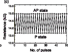
Magnetization reversal by voltage has been experimentally demonstrated in magnetic tunnel junctions (MTJs) using short voltage pulses, typically lasting between 0.5 ns and 2 ns. When a voltage is applied, a current flows through the MTJ, inducing spin-transfer torque (STT see here). However, a key distinguishing feature of voltage-induced magnetization reversal is that it can also occur in thicker MTJs, where the current is so low that the contribution of STT becomes negligible. This highlights that the mechanism behind voltage-induced reversal differs from that of current-induced reversal, operating effectively even when STT is insignificant. Voltage - induced magnetization reversal can be used as a recording mechanism for MRAM. The low power consumption for data recording is the main merit of use of VCMA effect for MRAM recording.

![]() (puzzle of VCMA reversal): It should be noted that in all measured nanomagnets, the gate-voltage-induced change in the anisotropy field does not exceed a few percent, which is insufficient to directly cause magnetization reversal. However, magnetization reversal remains possible in a MTJ made of similar nanomagnets using short pulses. This strongly suggests that parametric magnetization reversal (see here and here) is the primary mechanism for magnetization reversal by gate voltage in these nanomagnets. As a resonant mechanism, parametric magnetization reversal does not require a large change in the anisotropy field; typically, a few percent is sufficient.
(puzzle of VCMA reversal): It should be noted that in all measured nanomagnets, the gate-voltage-induced change in the anisotropy field does not exceed a few percent, which is insufficient to directly cause magnetization reversal. However, magnetization reversal remains possible in a MTJ made of similar nanomagnets using short pulses. This strongly suggests that parametric magnetization reversal (see here and here) is the primary mechanism for magnetization reversal by gate voltage in these nanomagnets. As a resonant mechanism, parametric magnetization reversal does not require a large change in the anisotropy field; typically, a few percent is sufficient.

 (merit of VCMA reversal for MRAM recording): One of the main advantages of magnetization reversal by voltage in MRAM applications is its low power consumption. This is because the reversal can occur in MTJs with thick MgO barriers that exhibit high resistance under minimal current. However, the primary challenge remains reducing the write-error rate to a level suitable for commercial MRAM applications, an issue that has not yet been fully resolved (See Refs. R6 & R8 here
![]() ).
).
 A brief history of the experimental demonstration of magnetization reversal by voltage:
 The first demonstration of magnetization reversal by voltage was reported in 2011 by Prof. Suzuki’s group from Osaka University (Refs. R1 & R2 here![]() ). Independent confirmations followed in 2016, with reports from Tohoku University (Ref. R3 here
). Independent confirmations followed in 2016, with reports from Tohoku University (Ref. R3 here![]() ) and UCLA (Ref. R4 here
) and UCLA (Ref. R4 here![]() ). Around this time, several major MRAM companies began testing voltage-driven magnetization reversal as a key mechanism for MRAM recording. While most of these results were shared at conferences, there are published reports from Toshiba (Ref. R5 here
). Around this time, several major MRAM companies began testing voltage-driven magnetization reversal as a key mechanism for MRAM recording. While most of these results were shared at conferences, there are published reports from Toshiba (Ref. R5 here![]() ) , Western Digital (Ref. R7here
) , Western Digital (Ref. R7here![]() ) and IMEC (Ref. R9here
) and IMEC (Ref. R9here![]() )
)
 Key features and properties of experimentally observed magnetization reversal by voltage:
![]() (feature 1): Occurrence in MTJs only
(feature 1): Occurrence in MTJs only
Magnetization reversal by voltage has been demonstrated exclusively in magnetic tunnel junctions (MTJs), but not in standalone nanomagnets.
![]() (feature 2): Distinguishing from STT mechanism:
(feature 2): Distinguishing from STT mechanism:
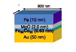
Since VCMA-type magnetization reversal occurs in MTJs where current flows under applied voltage, distinguishing it from Spin Transfer Torque (STT) reversal is crucial. The key differentiator is the use of high-resistance MTJs, where the current is so low that the STT contribution becomes negligible. For example, STT-induced reversal typically occurs in MTJs with MgO thicknesses between 0.8 to 1.2 nm. In thicker MgO layers, STT reversal is impossible due to MgO breakdown before reaching the critical current for reversal. VCMA-based reversal, however, has been observed in MTJs with thicker MgO, such as 1.5 nm (Ref. R1 here![]() ), 2.0 nm (Ref. R2 here
), 2.0 nm (Ref. R2 here![]() ), and even 2.8 nm (Ref. R3 here
), and even 2.8 nm (Ref. R3 here![]() ). Since tunnel resistance increases exponentially with MgO thickness, the STT effect is negligible in such devices.
). Since tunnel resistance increases exponentially with MgO thickness, the STT effect is negligible in such devices.
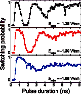
![]() (feature 3): Reversal by short pulses:
(feature 3): Reversal by short pulses:
Magnetization reversal occurs only when a short voltage pulse, typically ranging from 0.5 ns to 2 ns, is applied. Continuous (DC) voltage does not induce magnetization reversal.
![]() (feature 4): Polarity dependence:
(feature 4): Polarity dependence:
The reversal is triggered only by a negative voltage pulse; a positive pulse has no effect on magnetization reversal.
![]() (feature 5): Toggle-like behavior:
(feature 5): Toggle-like behavior:
Each successive pulse reverses the magnetization to the opposite state, regardless of the initial magnetization direction.
![]() (feature 6): External in-plane magnetic field required:
(feature 6): External in-plane magnetic field required:
Magnetization reversal by voltage only occurs when an external in-plane magnetic field is applied.
 Primary Challenge for commercial MRAM applications
The primary challenge for voltage- driven recording remains reducing the write-error rate to a level suitable for commercial MRAM applications, an issue that has not yet been fully resolved (Refs. R6 & R8 here![]() ).
).
The primary challenge with voltage-driven magnetization reversal is that, on very rare occasions (e.g., once in a million cycles), the nanomagnet’s magnetization either fails to reverse or reverses twice, returning to its initial state. This issue is likely related to the resonance-based (parametric) mechanism underlying voltage-driven magnetization reversal. Although such recording errors are infrequent, it is still large for commercial MRAM applications. This limitation currently hinders the full implementation of voltage-driven magnetization reversal in commercial MRAM.
This method may be only effective if the origin of the VCMA is related to the change of the Fermi level in ferromagnetic metal by the gate voltage. The Work-Function Engineering may optimize the Fermi energy in the metal at energy, where a smallest modulation of the position of the Fermi energy causes the largest modulation of the density of states of d-electrons (See below for details)
The strength of the PMA depends on the orbital deformation of iron and oxygen atoms at the metal-gate interface (See details here). Due to the orbital deformation these atoms experiences a large spin-orbit (SO) interaction (See details here and here). The gate voltage modifies such deformation and therefore it modifies the PMA. This fact is independent on the origin of the VCMA. The chemistry of the interface should be optimized such that the deformation of orbitals by the electrical field of the gate voltage should cause the largest change of the strength of the spin-orbit interaction and consequently the largest change of the PMA.
This method is independent on the origin of the VCMA. In the case of the shorter penetration depth, the electrical field of the gate voltage at the interface is large and its influence on the PMA is larger.
The more localized the d-electrons ( or f-electrons) are, the sharper their corresponding peak in DOS is. The VCMA is enlarged in the case when the Fermi level is at a slope of this peak. The VCMA is is larger, when the DOS of the localized electrons has a greater slope near the Fermi level. See Work-Function Engineering below for more details.
![]() In the case if the origin of VCMA effect is related to the gate-voltage modulation of the Fermi energy at the interface of a metal, the strength of the VCMA should depend on the metal material of the buffer layer. As Feb. 2019, I have measured several near-identical samples, where either Ta or W is used as the buffer. It is hard to make a clear conclusion, because other magnetic properties of a nanomagnet substantially depends on the material of the buffer.
In the case if the origin of VCMA effect is related to the gate-voltage modulation of the Fermi energy at the interface of a metal, the strength of the VCMA should depend on the metal material of the buffer layer. As Feb. 2019, I have measured several near-identical samples, where either Ta or W is used as the buffer. It is hard to make a clear conclusion, because other magnetic properties of a nanomagnet substantially depends on the material of the buffer.
![]() In the case if the origin of VCMA effect is related to the gate-voltage modulation of the Fermi energy at the interface of a metal, in ferromagnetic-metal/non-magnetic-metal super lattice the strength of the VCMA should depend on the metal material of the non-magnetic metal. A FeB/W multi layer is a good candidate to test such dependence. The VCMA strength is substantially depends on the W thickness in this multi layer. The VCMA may be either substantially enhanced or substantially suppressed depending on the W thickness. However, since other magnetic parameters also depend substantially on the W thickness, it is hard to make a clear conclusion.
In the case if the origin of VCMA effect is related to the gate-voltage modulation of the Fermi energy at the interface of a metal, in ferromagnetic-metal/non-magnetic-metal super lattice the strength of the VCMA should depend on the metal material of the non-magnetic metal. A FeB/W multi layer is a good candidate to test such dependence. The VCMA strength is substantially depends on the W thickness in this multi layer. The VCMA may be either substantially enhanced or substantially suppressed depending on the W thickness. However, since other magnetic parameters also depend substantially on the W thickness, it is hard to make a clear conclusion.
Note: A thick bcc W/FeB multilayer has substantial PMA. Their properties are similar to a fcc Co/Pt multilayer. Note: A W/FeB multilayer with a thick W layer (1-2 nm) has a greater VCMA effect than that in a FeB film. A W/FeB multilayer with a thin W layer (0.1-0.5 nm) has a small VCMA effect. Note: Both crystal and magnetic properties of FeB/W multi layers are influenced substantially by the thickness of the W layer.
Main idea: To turn the Fermi level in a ferromagnetic metal to the position where the VCMA is the largest.
Band of model of d-electron and the VCMA effect |
|||||||||
|
|||||||||
click on image to enlarge it |
According to the band model, the electron are extended over the whole crystal. Their states are distinguished by their energies in bands with a continuous and broad spectrum and a nearly- constant density of state.
The localized electron states are localized in the vicinity of an atomic site. The energy spectrum of localized electrons consists of narrow lines.
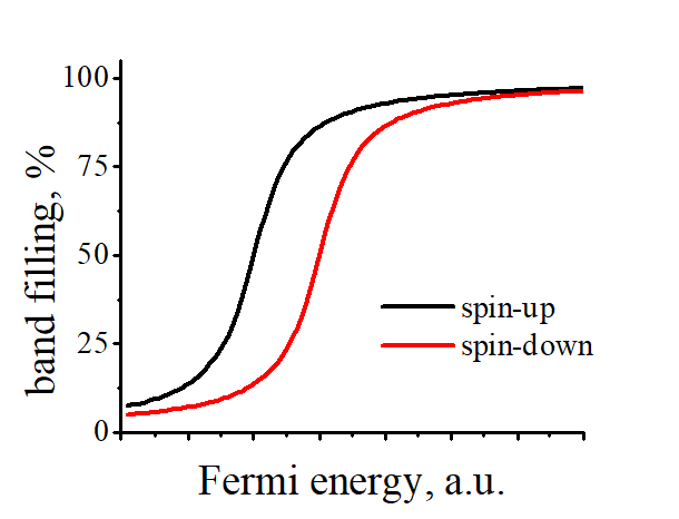
Filling of spin-up and spin-down bands: Figure p1 shows the amount of filling of one d-band as function of the position of the Fermi energy. At a lower energy the d-band is not filled at all. At a higher energy the band is fully filled. Since the magnetic energy is different for spin-up and spin-down electrons in intrinsic magnetic field, which exists inside of the ferromagnetic metal, the filling of the spin-up and spin-down band are different. At first, the spin-up bands is filled and always there are more spin-up than spin-down electrons.
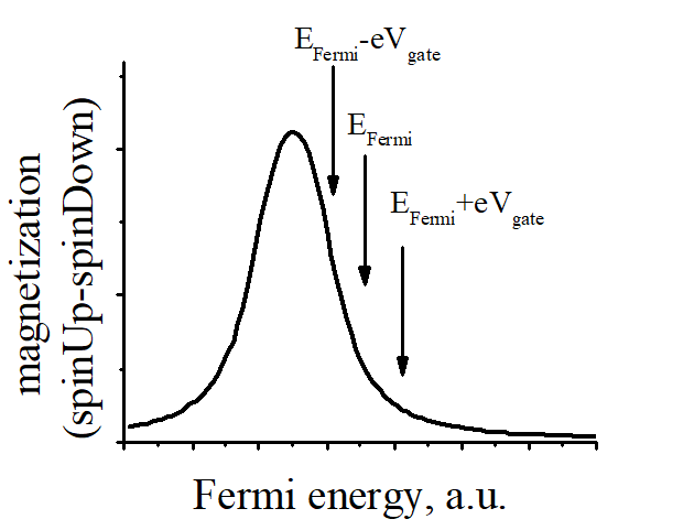
![]() Magnetization vs the position of the Fermi energy. The magnetization is difference between number of spins of the spin-up and spin-down electrons. Figure p2 shows the magnetization, which is calculated from Fig. p1.
Magnetization vs the position of the Fermi energy. The magnetization is difference between number of spins of the spin-up and spin-down electrons. Figure p2 shows the magnetization, which is calculated from Fig. p1.
The magnetization-modulation mechanism can be enhanced in the case of a presence of a sharp peak in the DOS of a ferromagnetic metal near the Fermi level. This fact can be explained as follows. The magnetization change dM under a gate voltage can be calculate as
where dEFermi is the change of the Fermi level, M(E) is the dependence of the magnetization on the Fermi level. The![]() is larger, when the DOS of the localized electrons has a greater slope near the Fermi level.
is larger, when the DOS of the localized electrons has a greater slope near the Fermi level.
From Eq. (p1), the change of the magnetization dM is the largest, when the ![]() is the largest. From Fig.3p it is the case when the Fermi level at the steepest slope of the M(E) (Fig.p3).
is the largest. From Fig.3p it is the case when the Fermi level at the steepest slope of the M(E) (Fig.p3).
Not at all. From Fig.p3, the VCMA effect is the smallest at the energy, at which the magnetization is the largest.
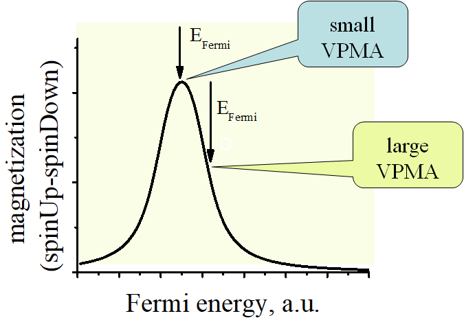
Work function engineering of magnetic properties of a metal |
||||||
|
||||||
click on image to enlarge it |
To move the Fermi energy to a position where the VCMA is the largest.
The VCMA is the largest at the slope of the peak of Fig. p3, where ![]() is the largest.
is the largest.
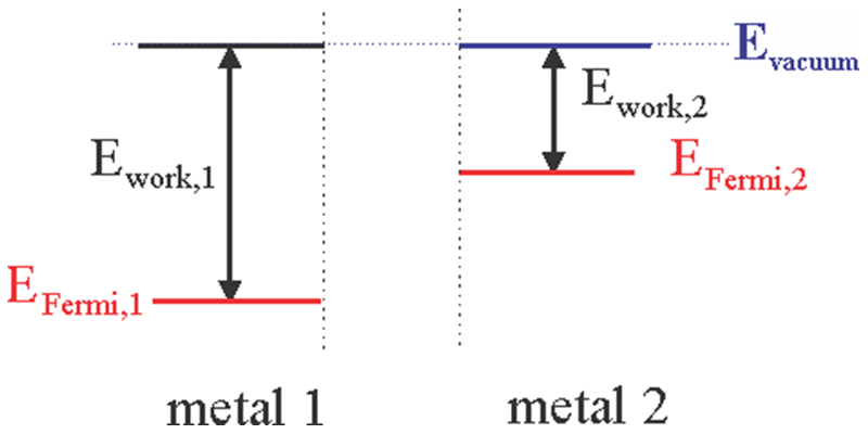
There is a charge accumulation at a contact between two metal. In the narrow region of the charge accumulation, the position of the Fermi level changes from its bulk position.
Each metal has a different work-function energy. The work-function energy is the energy from the Fermi energy in the metal to the vacuum energy (fig. p4). When two of different are in contact, some electrons moved from one metal to another in order to make the Fermi energy the same in both metals. In the region of the charge accumulation the position of the Fermi energy is different comparing to its bulk position.
The thickness of the charge accumulation region is about the length of a conduction electron or the same the mean-free path λmean (See here for details)
Any external charge in the electron is screened (See Electron screening )by conduction electron within the Debye length. The case in the vicinity of the interface between two metals is different. Some conduction electrons are reflected by the interface. It changes the transport and screening properties of conduction electrons. Also, it forms a region of a charge accumulation (See details here).
Yes. However, in this case the Fermi energy should be moved to the top of peak of Fig p3 instead of the steepest slope.
A. It is moderate. The spins of conduction electrons is not major contribution to the magnetization. The contribution of the d-electrons is the major contribution. However, the contribution of the conduction electrons is not negligible as well. It can be estimated from the known energy distribution of spin polarized electrons and density of states of the conduction electrons. See here for more details.
![]() Are the d-electrons in a ferromagnetic metal the delocalized (band-type) or the localized?
Are the d-electrons in a ferromagnetic metal the delocalized (band-type) or the localized?
![]() The d-electrons in a ferromagnetic metal are localized with some weak band-type features.
The d-electrons in a ferromagnetic metal are localized with some weak band-type features.
More details see here
A. Not much. The d-electrons have some component of sp- spacial symmetry, but still the d-electrons remain fully localized. (Nearly similar as it would not be any hybridization). The conduction electrons have some component of d- spacial symmetry, but the conduction electrons remain fully delocalized. Any electron is either localized (electron length is short) or delocalized (electron length is long). An electron cannot have simultaneously one short part and one long part.
A. This question is still under debate. Some ab-initial calculations suggest that the d-electrons of et symmetry are localized, but the d-electrons of t2g symmetry are delocalized. As Feb.2019, it is only a suggestion.
A. It is possible, but it have not been verified experimentally yet. It would be a very interesting case if the conduction electrons consist of electrons of very different symmetries: the sp-symmetry and d- (t2g )symmetry . It would be similar to the case of a semiconductor where conduction electrons of two very different symmetries can coexist: electrons (s-symmetry) and holes (p-symmetry). (See here for details).
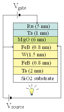
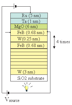
VCMA in FeB/W multilayers & FeB layer |
||
|
||
|
||
|
||
| Material of ferromagnetic layer: (top) FeB (1.1 nm) ; (middle) FeB(0.8 nm)/W (1.5nm)/FeB(0.8 nm); (bottom) [FeB(0.68 nm)/W (0.25 nm)]4 | ||
| Fig. 31 The voltage dependence of the coercive field in FeB/W multilayers & FeB layer. Click on image to enlarge it. |
Note: A thick bcc W/FeB multilayer has substantial PMA. Their properties are similar to a fcc Co/Pt multilayer.
Note: A W/FeB multilayer with a thick W layer (1-2 nm) has a greater VCMA effect than that in a FeB film. A W/FeB multilayer with a thin W layer (0.1-0.5 nm) has a small VCMA effect.
Note: Both crystal and magnetic properties of FeB/W multi layers are influenced substantially by the thickness of the W layer.
Influence on the crystal quality: At a thinner W layer, the multi layer becomes rougher. As the result, the VCMA strength decreases. At the W thickness of 0.2 nm and thinner, the multi layer surface becomes too rough so that the FeB becomes not-continuous and consequently it changed to be paramagnetic.
Influence on the magnetic properties: The strength and the polarity of the exchange coupling between FeB layers depend substantially on the thickness of the W layer. I have not checked the full dependence of the exchange coupling on the W thickness. However, the measured magnetization of FeB/W multilayer is smaller that that of FeB It implies the exchange coupling might be anti ferromagnetic.
The Work-Function Engineering may enhance the VCMA effect only if the modulation of the Fermi energy at metal/oxide interface is the main origin of the VCMA effect.
![]() In the case if the origin of VCMA effect is related to the gate-voltage modulation of the Fermi energy at the interface of a metal, the strength of the VCMA should depend on material of the gate metal. As Feb. 2019, I have measured several samples with Ta and W gates. However, I have not found any clear dependence of VCMA on the material of the gate metal.
In the case if the origin of VCMA effect is related to the gate-voltage modulation of the Fermi energy at the interface of a metal, the strength of the VCMA should depend on material of the gate metal. As Feb. 2019, I have measured several samples with Ta and W gates. However, I have not found any clear dependence of VCMA on the material of the gate metal.
It is only possible to detect the dependence of the VCMA on the material of the gate metal if the Fermi level is not pinned or partially pinned inside the gate oxide. It still a challenging task to fabricate the gate oxide of the required quality.
different buffer layer |
Excess of oxygen at gate/metal interface |
Possible explanation of polarity change |
 |
 |
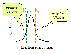 |
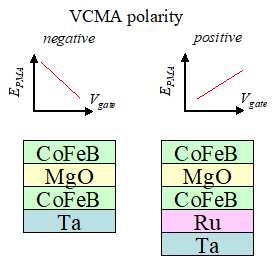
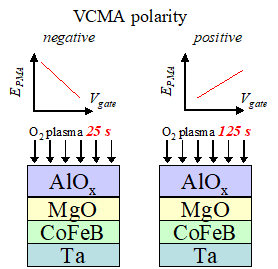
Fig. 24(a) Adding 1a 1-nm Ru layer to buffer reverses the polarity of VCMA |
Fig. 24(b) A long exposure of AlOx in oxygen plasma reverses the polarity of the VCMA. | Fig. 24 (c)If there is a sharp peak in DOS in CoFeB, dM/dE has different signs at different sides of peaks. Therefore, the change of the Fermi level in CoFeB may cause the sign change of VCMA (See Eq.1) |
Case 1: different buffer layer
It was experimentally demonstrated that the insertion of a Ru layer between CoFeB and Ta changes the polarity of the VCMA effect
possible explanation 1: The insertion of the Ru changes the position of the Fermi level at the CoFeB/MgO interface.
possible explanation 2: The crystal quality of the CoFeB/MgO interface degrades due to insertion of the Ru layer. As a result, the type of oxygen-iron bonding is slightly changed, which leads to the change of the PMA and the VCMA
Case 2 Excess of oxygen at gate/metal interface
It was experimentally demonstrated that a longer exposure of AlO in oxygen plasma changes the polarity of the VCMA effect.
In the case of a longer plasma exposure, the amount of oxygen at the CoFeB/MgO interface. It is known that the PMA at the CoFeB/MgO interface substantially depends on the amount of oxygen at it (![]() ). In the case of the gate oxide of Fig.24(b), the VCMA mechanism is oxide diffusion in the gate, which is influence by initial amount of oxygen at the interface.
). In the case of the gate oxide of Fig.24(b), the VCMA mechanism is oxide diffusion in the gate, which is influence by initial amount of oxygen at the interface.
Influence of quality of gate oxide on a VCMA measurement |
|||||||
|
|||||||
The defects in the MgO gate were characterized DLTS and DLCS. click on image to enlarge it. |
The fabrication of a high-quality oxide is critically important in order to obtain a strong VCMA effect.
I have developed a growth method of MgO to fabricate a high-quality gate with a high break-down voltage (0.8-1 V/nm) and a low-density of defects.
The defects in the MgO gate were characterized and measured using the capacitance-voltage measurements, DLTS (deep level transition spectroscopy) and DLCS (deep level conduction spectroscopy).
![]() 1. The Fermi level can be pinned inside the gate oxide. In this case, the applied voltage at the gate/metal interface is substantially reduces. That causes the reduction of VCMA.
1. The Fermi level can be pinned inside the gate oxide. In this case, the applied voltage at the gate/metal interface is substantially reduces. That causes the reduction of VCMA.
![]() 2. Oxygen ions diffuses in a gate oxide with defects under a gate voltage. The PMA at an Fe/oxide or Co/oxide interface increases when there are more oxygen ions at interface. That causes a substantial modulation of the PMA. It is undesirable effect, because its very slow response.
2. Oxygen ions diffuses in a gate oxide with defects under a gate voltage. The PMA at an Fe/oxide or Co/oxide interface increases when there are more oxygen ions at interface. That causes a substantial modulation of the PMA. It is undesirable effect, because its very slow response.
![]() 3. The electrons can be capture into deep defect levels in the gate oxide. These electrons are slowly released under an opposite gate voltage. The captured electrons modify the distribution of the electrical field in the gate oxide and correspondingly the voltage applied to the oxide/ferromagnetic-metal interface.
3. The electrons can be capture into deep defect levels in the gate oxide. These electrons are slowly released under an opposite gate voltage. The captured electrons modify the distribution of the electrical field in the gate oxide and correspondingly the voltage applied to the oxide/ferromagnetic-metal interface.
A. It is very difficult and often impossible. For example, the measurement becomes dependent on the time constant of measurement. Such measurements are very confusing. Additionally, the hysteresis loop of Fig.22 (b), which is also may be observed for different voltage-dependent parameters, can completely overlap the intrinsic properties of the VCMA effect.
A. For the fabrication of the gate oxide the thermo-oxidation of Si or the atomic layer epitaxy (ALE) is often used. These technologies yields a very high quality of the gate oxide. It is still challenging to apply the similar technologies for the studied VCMA devices. Mainly, the sputtering of the oxide is used. In this case, the quality of the gate oxide is moderate. I have tried the sputtering of different oxides: MgO, Al2O3, MgO+SiO2. In each case, it is possible to obtain acceptable quality and to measure the VCMA. However, the quality is still very far from the best. The fabrication of the high-quality of the gate oxide is still a challenging task in the field.
Several condition should be satisfied:
![]() The ferromagnetic metal should not be oxidized or the oxidation should be controllable. It can be achieved at a low growth temperature.
The ferromagnetic metal should not be oxidized or the oxidation should be controllable. It can be achieved at a low growth temperature. ![]() the surface of gate oxide should smooth. It can be achieved at a high growth temperature, when the mobility of atoms on the surface is high.
the surface of gate oxide should smooth. It can be achieved at a high growth temperature, when the mobility of atoms on the surface is high. ![]() The growth initialization should be 2d-type (not 3D-type). It can be achieved by suppressing atom mobility at a low temperature.
The growth initialization should be 2d-type (not 3D-type). It can be achieved by suppressing atom mobility at a low temperature. ![]() The number of defects in gate oxide should be low. It can be achieved at a higher growth temperature. Also, the metal - oxygen ratio should be optimized.
The number of defects in gate oxide should be low. It can be achieved at a higher growth temperature. Also, the metal - oxygen ratio should be optimized.
My method to optimize the crystal quality of the sputtered MgO:
At first, a 1 nm MgO was deposited at room temperature, next the sample was annealed at 220 deg C for 30 minutes and the remaining of the MgO gate oxide was grown at 220 deg C. Three 30-minute growth interruptions after each 1 nm of growth were used to improve the MgO crystal quality.
Voltage-dependence of left and right edges of the coercive loop |
|||||
|
|||||
click on image to enlarge it. |
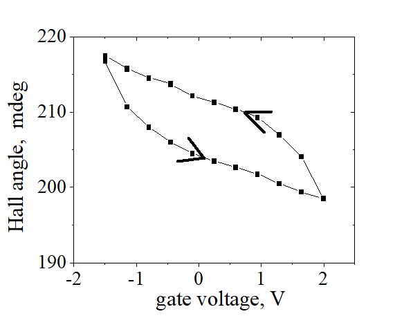
A coercive loop has two switching points: (1) from magnetization-up to magnetization-down; (2) from magnetization-down to magnetization-up. In the case of the SOT effect these two magnetization switchings are affected differently by the SOT effect.
![]() A. No. Both switchings are absolutely identical and their voltage-dependence is the same
A. No. Both switchings are absolutely identical and their voltage-dependence is the same
Why there is a slight offset between spin down-to-up and up-to-down switchings in Fig.11(a)?
It is because the size of nucleation domain for magnetization switching depends slightly on the magnetization switching direction (See here for more details)
VCMA vs Hc & HanisThe dependence has not been found |
||||||
|
||||||
Two devices, which were fabricated on different parts of wafer, have substantially different Hc, because a slight variation of FeB thickness between edge and center of the wafer. However, the slope of the voltage-dependence of Hc is the same for them. This coincidence represents a general tendency. |
||||||
| Note: The thickness variation can be controlled by a variation of sample rotation speed during growth and the the sample distance from the sputtering target. The variation of thickness of this wafer has been made intentionally large. | ||||||
| click on image to enlarge it. |
The coercive and anisotropy fields may be substantially different for devices fabricated on different sides of the same wafer due a slight variation of the thickness of the ferromagnetic metal. However, in case if the quality of the gate oxide remains the same, the measured VCMA is identical for such sample despite of a substantial difference of their Hanis and Hc.
![]() It implies that the strength of the VCMA might not depended on absolute values Hanis and Hc. Note :
It implies that the strength of the VCMA might not depended on absolute values Hanis and Hc. Note :
Thicker FeB: Hc-> larger; Hanis-> larger; retention time ->larger; nucleation domain size->the same
Thinner FeB: Hc-> smaller; Hanis->smaller; retention time ->smaller; nucleation domain size->the same
![]() How large is the possible variation of the FeB thickness?
How large is the possible variation of the FeB thickness?
![]() From ~0.8 nm to ~1.2 nm. The magnetization of a thicker film becomes in-plane. A thinner film becomes a paramagnetic.
From ~0.8 nm to ~1.2 nm. The magnetization of a thicker film becomes in-plane. A thinner film becomes a paramagnetic.
![]() Can the thickness of a ferromagnetic FeB film be thinner than 0.8 nm? Is it possible to grow such a thin ferromagnetic FeB film?
Can the thickness of a ferromagnetic FeB film be thinner than 0.8 nm? Is it possible to grow such a thin ferromagnetic FeB film?
![]() Using a direct growth it is impossible. At the beginning of the FeB growth, the clusters of FeB is formed, they are not connected, the FeB is not continuous film and it is paramagnetic. When the growth proceeds, the clusters collapse and form a continuous smooth film, which becomes ferromagnetic.
Using a direct growth it is impossible. At the beginning of the FeB growth, the clusters of FeB is formed, they are not connected, the FeB is not continuous film and it is paramagnetic. When the growth proceeds, the clusters collapse and form a continuous smooth film, which becomes ferromagnetic.
In order to fabricate a smooth continuous ferromagnetic film the following advanced growth procedure should be used:
step 1: growth of a thicker FeB film (~1.5-2.5 nm)
step 2: Ar milling of FeB film down to the designed thickness
step 3: proceeding of the growth of the remaining of the film
The ferromagnetic FeB film of thickness ~0.1-0.2 nm can be fabricated by this method. The magnetization of such film is perpendicular-to-plane. The thickness of the FeB can be evaluated by this method.
![]() Does the film roughness influence the VCMA?
Does the film roughness influence the VCMA?
![]() A. Both the PMA and VCMA are influenced by the film roughness very much. It is hard to show it in numbers. However, this fact is very obvious. The VCMA of a rougher film is smaller. See for example Fig.31 here.
A. Both the PMA and VCMA are influenced by the film roughness very much. It is hard to show it in numbers. However, this fact is very obvious. The VCMA of a rougher film is smaller. See for example Fig.31 here.
VCMA vs sample thickness |
||||||
|
||||||
The assumption that the VCMA is stronger in a thinner layer is not valid for these samples. |
||||||
| click on image to enlarge it. |
A. No.
A. The film thickness may influence the VCMA only when the penetration depth of the gate electrical field into the ferromagnetic field becomes comparable to the film thickness. Also, such influence strongly depends on the main origin of the VCMA. It is clear that the VCMA is an effect of an interface, but not of bulk of material. Only some influence of film thickness on the interface properties may change the VCMA.
A. It is very hard to estimate. It may varies from a material to a material. Also, it should depend substantially on the type and density of the surface states at the metal oxide-interface. Maybe it could be estimated from the capacitance-voltage measurements or DLTS (deep level transition spectroscopy) or DLCS (deep level conduction spectroscopy) measurements. As Feb. 2019 I do not know any report on a successful measurement of the penetration depth. My suggestion is that the penetration depth is about 0.01-01 nm.
![]() The gate voltage affects the ferromagnetic metal only in a very thin region of the gate oxide, which is very close to the gate oxide.
The gate voltage affects the ferromagnetic metal only in a very thin region of the gate oxide, which is very close to the gate oxide.
|
|||||
|
|||||
|
1. 1st demonstration
A gate voltage is applied to magnetic wire through electrolyte. The change of coercive field under the gate voltage was detected
2. 1st solid-state device (practical device)
3. 1st high-speed voltage-induced magnetization reversal
It is a breakthrough result in the field, because it opened a possibility of the fabrication of a new type of high-speed low- power- consumption magnetic random access memory (MRAM)
A. I guess there are several contributions to the bias-dependence of TMR. The voltage dependence may have some contribution. However, it should be a contribution, which is polarity dependent. The voltage-control change of the spin polarization always changes its sign, when the voltage polarity is reversed. I have checked many samples already. The spin polarization always linearly increases under a negative gate voltage and it always linearly decrease under a positive gate voltage.
Publications
Intermag (Singapore) March 2018![]() presentation
presentation
SSDM (Tokyo) Sep. 2018 ![]() presentation and
presentation and ![]() abstract
abstract
![]() long version of manuscript. July 14, 2018 &
long version of manuscript. July 14, 2018 &

| Intermag 2023. Sendai, Japan | The 67th Annual Conference on Magnetism and Magnetic Materials (MMM 2022) | |
|---|---|---|
 |
 |
|
| click on image to see Youtube Video | click on image to see Youtube Video | |
| (title): Systematic study of the strength of VCMA effect in nanomagnets of small and large strength of spin-orbit interaction. | (title:) Modulation of spin-orbit interaction by a gate voltage. VCMA effect |
![]() Recently, I read a research article (See link here) and I felt a huge confusion. In the article, the authors said that, 'the SO interaction depends on an orthogonality between the applied electric field, the equilibrium magnetization, and the wave vector of the spin waves'. Their main observation is that, when the External Electric field and Equilibrium magnetic field are orthogonal, then they observed spin orbit coupling (they applied out of plane E field). But when they changed E field direction in plane, they didn't observe the spin orbit coupling. Actually, this makes me confused. It makes some queries in my mind: 1. Is it mandatory of being orthogonal of both E field and magnetization for observing E field driven spin orbit interaction? 2. If needed, what is the reason or facts?
Recently, I read a research article (See link here) and I felt a huge confusion. In the article, the authors said that, 'the SO interaction depends on an orthogonality between the applied electric field, the equilibrium magnetization, and the wave vector of the spin waves'. Their main observation is that, when the External Electric field and Equilibrium magnetic field are orthogonal, then they observed spin orbit coupling (they applied out of plane E field). But when they changed E field direction in plane, they didn't observe the spin orbit coupling. Actually, this makes me confused. It makes some queries in my mind: 1. Is it mandatory of being orthogonal of both E field and magnetization for observing E field driven spin orbit interaction? 2. If needed, what is the reason or facts?
To grasp the concept of how a gate voltage affects the spin waves, it's crucial to have a clear understanding of spin-orbit interaction.
The spin- orbit interaction describes a magnetic field of relativistic origin and nothing else. This magnetic field Hso of spin- orbit interaction possesses unique properties and characteristics.Once you comprehend these features, it will be easier for you to understand any effect related to spin- orbit interaction.
(feature 1 of SO) The direction of the magnetic field Hso of spin- orbit interaction consistently aligns with the direction of the total magnetic field Htotal applied to the electron orbital. Hso is linearly proportional to Htotal. The proportionality coefficient is called the coefficient kso of spin- orbit interaction. The method for measuring kso is relatively straightforward. I have been doing measurements of kso for many years now.
Inside a ferromagnetic film, Htotal is referred to as the internal magnetic field, comprising the sum of the magnetic field along the magnetization M and the demagnetization field Hdemag. Hso approximately tracks M with some deviation attributable to Hdemag.
(feature 2 of SO): The strength of the spin-orbit interaction (SO) is proportional to the orbital deformation. kso is substantially larger when Htotal is directed along the deformation compared to when it is perpendicular to the deformation.
When an electric field is applied, the orbital is deformed along the electrical field, leading to an increase in kso. This effect is referred to as the Voltage-Controlled Magnetic Anisotropy (VCMA) effect.
In the case of a metal, the voltage is applied only to the interface, deforming the orbital there and modulating Hso only for interface orbitals. In the case of a dielectric material (like a garnet), the voltage is applied through the bulk of the film, modulating Hso for orbitals in the bulk.
(spin waves): In the dynamic LL equation for spin waves, it is necessary to include Hso and its modulation by the gate voltage. I believe that considering this modulation of spin-orbit interaction by the gate voltage will provide a comprehensive explanation of the properties of spin waves.
(about paper) I am confident that the correct description of the spin-orbit interaction (SO), as explained above, accounts for all the observed experimental features of the spin waves.
(about direction of applied electrical field)
Absolutely not. To measure the gate-voltage modulation of kso and for magnetization reversal induced by a gate voltage, an in-plane bias magnetic field is necessary. The VCMA effect exhibits similar strength in this scenario. This fact is undeniable.
 Questions about magnetization reversal by a gate voltage
That's correct. The maximum change in anisotropy field due to gate voltage, measured in FeB and FeCoB nanomagnets, does not exceed 10-20%. This small change is insufficient for direct magnetization reversal by a gate voltage. However, magnetization reversal is still possible in these nanomagnets using short pulses. This strongly suggests that the parametric magnetization reversal mechanism is the primary means of magnetization reversal by gate voltage. As a resonance mechanism, parametric magnetization reversal does not require a large change in the anisotropy field; typically, a few percent is sufficient. Another indication that parametric magnetization reversal is the mechanism at play is the essential requirement for magnetization tilting by an external in-plane magnetic field to achieve magnetization reversal by gate voltage. This requirement is consistent with the parametric magnetization reversal mechanism, which also depends on such tilting. Without it, parametric magnetization reversal through modulation of the anisotropy field is impossible. To the best of my knowledge, magnetization reversal by gate voltage has only been observed in the presence of an external in-plane magnetic field, further pointing to the parametric mechanism as the likely explanation.
The observed voltage-induced changes of H0 and Kso are not small when considering a resonance-based mechanism for magnetization reversal. I believe the parametric mechanism is likely the key process behind the experimentally observed magnetization reversal by a short voltage pulse. All the experimentally observed characteristics of magnetization reversal by a short voltage pulse, as outlined above, align well with the properties and conditions required for the parametric reversal mechanism. These features strongly support the hypothesis that parametric resonance is the underlying process driving the voltage-induced magnetization reversal.
I fully understand your concern regarding how a small change in anisotropy due to a pulse voltage can lead to magnetization reversal. Another concern might be why VCMA-type magnetization reversal only occurs under very specific conditions, as I mentioned above, whereas STT-type reversal simply happens once the current reaches a critical threshold.
The key to addressing these concerns lies in the resonance nature of the VCMA reversal. In a resonance effect, even a small disturbance can produce a significant impact. For instance, a slight but periodic push can dramatically increase the amplitude of a swing. Similarly, the synchronized steps of soldiers marching across a bridge can cause structural failure, an outcome that wouldn’t occur without resonance. In the case of VCMA, the voltage-induced resonance change in anisotropy amplifies the magnetization precession angle, leading to magnetization reversal under specific conditions.
While the exact solution for parametric magnetization reversal is quite complex—requiring the nonlinear precession dynamics to be solved using Landau-Lifshitz equations—the basic concept behind the resonance mechanism can be understood similarly to those simpler examples I mentioned before. Even though the math is tricky, the essence of how a small, periodic influence can lead to a significant effect still holds true here.
I agree with your point that the modulation of magnetization may not be the dominant contributor to the observed gate-voltage modulation of magnetic anisotropy and the strength of spin-orbit interaction. The issue is not whether gate-voltage modulation of magnetization exists or doesn't exist—it undoubtedly does, as it is a consequence of fundamental physical principles.
The application of gate voltage modulates the Fermi level, which alters the filling ratio between spin-up and spin-down localized d-electrons, leading to a change in magnetization. This is an indisputable fact.
The key question, however, is whether the gate-voltage modulation of magnetization is a primary or secondary contributor to the VCMA effect. Given its fundamental origin, the modulation of magnetization can only occur with a specific polarity. The fact that the experimentally observed polarity of the VCMA effect aligns with this predicted polarity suggests that the gate-voltage modulation of magnetization is likely a major contributor to the VCMA effect. That being said, while this is a strong hypothesis, it remains an informed assumption, not a definitive conclusion.
I completely agree that multiple independent pieces of evidence are necessary to make an indisputable statement about the true origin of a complex effect like the VCMA effect. However, the fact that the measured polarity of the change in the anisotropy field coincides with the change expected from gate-voltage modulation of magnetization, and is opposite to the change expected from gate-voltage modulation of spin-orbit interaction, suggests that the gate-voltage modulation of magnetization is the largest contributor to the VCMA effect.
It's important to emphasize that the polarity of gate-voltage modulation of magnetization is inherently and fundamentally fixed. This is because ferromagnetism can only exist when the d-orbitals are more than half-filled, as is the case with Fe, Co, and Ni. Since the spin-up states are already filled, any charge accumulation or depletion affects only the spin-down electrons. Consequently, charge accumulation always increases the number of spin-down electrons, thereby decreasing magnetization. Conversely, charge depletion decreases the number of spin-down electrons, which enlarges magnetization.
Although I do not generally believe in coincidences, as you pointed out, it is important to acknowledge the possibility that the observed polarity of gate-voltage modulation of the anisotropy field coinciding with the only possible polarity of gate-voltage modulation of magnetization could be just a coincidence, and that some other effect with the same polarity might be the major contributor to the VCMA effect.
I have measured only nanomagnets that remain in a single-domain state, ensuring consistent magnetization saturation without the formation of magnetic domains even without an external magnetic field. In this saturated state, the spins of localized electrons are aligned, and their quantity remains unchanged within the moderate magnetic fields applied. In contrast, the number of spin-polarized conduction electrons increases in response to an external magnetic field. When this field is aligned with the magnetization—and thus with the spin direction of spin-polarized electrons—the spins of initially spin-unpolarized electrons begin to align with the external field, effectively increasing the number of spin-polarized electrons. The increase of the number of spins aligned along magnetization, in turn, enhances the magnetization. This measurement is also used to estimate the spin polarization of the conduction electrons
The theoretical description of this process is straightforward and relatively simple. Importantly, this theoretical description is very well fitted to the experimental measurements. For further details, see my 2020 PRB paper here
(about my calculations on magnetic anisotropy): In Appendix of my AIP 2024 paper here, I have to describe the calculation of the magnetic anisotropy in as much detail as possible to facilitate ease of understanding. The calculations are based on fundamental time/space symmetries, without any approximations or simplifications, so I am confident in their accuracy.
(magnetization and magnetic anisotropy): I’m unclear about the source of your skepticism and I do not understand the reason why you have doubts. A stronger magnetization yields a higher internal magnetic field, which enhances spin-orbit interaction and, consequently, magnetic anisotropy. Experimentally, this relationship is also evident; when the magnetization of a nanomagnet decreases or vanishes, the anisotropy field similarly decreases or vanishes. However, in practice, variations in the strength of spin-orbit interaction and demagnetization fields tend to influence the anisotropy field more significantly than changes in magnetization.
The amount of ferromagnetic material in the nanomagnet is too small to be reliably measured using SQUID or any other conventional magnetometer.
Undoubtedly, the voltage-controlled magnetic anisotropy (VCMA) effect has multiple contributing factors. The observed opposite polarity of the voltage modulation of strengths of spin- orbit interaction and magnetic anisotropy is a clear proof. The modulation of magnetization may not be the dominant mechanism driving the observed gate-voltage dependence of magnetic anisotropy. However, the existence of gate-voltage-induced magnetization modulation is not in question—it is a direct consequence of fundamental physical principles.
The key question is whether this modulation of magnetization is a primary or secondary contributor to the VCMA effect. Notably, the polarity of gate-voltage-induced magnetization modulation is fundamentally fixed. This arises from the intrinsic nature of ferromagnetism, which requires more than half-filled d-orbitals, as is the case for Fe, Co, and Ni. Since the spin-up states are already occupied, any charge accumulation or depletion primarily affects the spin-down electrons. As a result, charge accumulation increases the number of spin-down electrons, leading to a reduction in magnetization, while charge depletion decreases the number of spin-down electrons, thereby enhancing magnetization.
Although I generally do not believe in coincidences, it is worth acknowledging the possibility that the observed polarity of gate-voltage modulation of the anisotropy field happens to match the only possible polarity of gate-voltage-induced magnetization modulation by chance. The fact that the experimentally observed polarity matches the only possible polarity of gate-voltage-induced magnetization modulation provides strong support for the suggestion that gate-induced magnetization modulation is the primary contributor to the VCMA effect.
With the available data, it is difficult to precisely estimate the magnitude of magnetization change. However, it is evident that the modulation of magnetization rapidly decays with increasing distance from the interface. The depth of this modulation should follow the penetration depth of the Fermi-level shift induced by gate voltage. To better understand this dependence, further experimental and theoretical investigations are needed.
At this stage, the critical question is whether magnetization modulation is a primary or secondary contributor to the VCMA effect. If it proves to be the dominant mechanism, additional research efforts should be directed toward quantifying its magnitude and underlying mechanisms.
Undoubtedly, the VCMA effect arises from multiple contributing factors. A key indication of this complexity is the observed opposite polarity of voltage modulation of spin-orbit interaction strength and magnetic anisotropy, which suggests the presence of multiple competing effects. While magnetization modulation may not be the dominant mechanism driving the observed gate-voltage dependence of magnetic anisotropy, its existence is unquestionable—it is a direct consequence of fundamental physical principles.
Notably, the polarity of gate-voltage-induced magnetization modulation is inherently fixed. This stems from the fundamental nature of ferromagnetism, which requires more than half-filled d-orbitals, as is the case for Fe, Co, and Ni. Since the spin-up states are already occupied, any charge accumulation or depletion primarily affects the spin-down electrons. Consequently, charge accumulation increases the number of spin-down electrons, reducing the overall magnetization, while charge depletion decreases the number of spin-down electrons, enhancing magnetization.
The fact that the experimentally observed polarity matches the only possible polarity of gate-voltage-induced magnetization modulation provides strong support for the suggestion that gate-induced magnetization modulation is the primary contributor to the VCMA effect.
(thickness dependence of VCMA)
Regarding thickness dependence, I have measured a large number of FeB and FeCoB nanomagnets with thicknesses ranging from 0.8 nm to 1.2 nm. However, no clear correlation between VCMA strength and magnetic layer thickness was observed. In future work, I plan to investigate this issue further by combining these measurements with two additional measurement techniques currently under development.
For further resources on spin-orbit interaction, perpendicular magnetic anisotropy (PMA), or measurement methods, please refer to these pages:
Measuring Spin-Orbit Interaction here:
(VCMA and Conduction Electrons): Experimentally, I have not observed any dependence of the VCMA effect on the properties of conduction electrons, nor am I aware of any compelling theoretical or experimental evidence supporting such an influence. The VCMA effect, like the related PMA effect, primarily involves localized electrons rather than conduction electrons.
(Conduction vs. Localized Electrons): Localized and conduction electrons exhibit notably different properties, largely due to the distinct scattering frequencies they experience. For instance, localized electrons are typically "quenched" (orbital moment = 0), while conduction electrons are "unquenched." It is important here that spin distributions of localized and conduction electrons differ significantly. The spins of localized electrons align primarily along or opposite the magnetization direction (spin-up and spin-down). In contrast, conduction electrons belong either to spin-polarized or spin-unpolarized groups. Spin-polarized electrons align their spins in one direction, while spin-unpolarized electrons have spins distributed uniformly across all directions. Because of frequent scatterings, the spins of conductions electrons are always mixed up. Notably, even spin-independent scattering events contribute to this spin-mixing. One example to illustrate this mixing: when spin-up and spin-down electrons are scattered into the same quantum state, the time-reversal symmetry (T-symmetry) of that state becomes unbroken. Consequently, when scattered out of this state, the electron spins can be found in various orientations (e.g., spin -left /spin -right or spin -front /spin -back, or any pair of opposite directions). This very frequent mechanism that occurs approximately every 100 fs at room T in a solid, mixes up the spins of conduction electrons.
Further details on this mechanism can be found here ( about spin polarization) or here (about spin rotation during spin- independent scaterings)
All experimentally observed properties of the family of magneto-transport effects (see here) align well with this spin distribution of conduction electrons containing two groups of spin-polarized and spin- unpolarized conduction electrons, which supports the correctness of such spin distribution for the conduction electrons.
(On the Rashba Effect:) The Rashba effect is observable only at extremely low temperatures, typically below 1 K, where electron scattering is minimal. At higher temperatures, separate distributions of spin-up and spin-down conduction electrons do not persist due to increased spin mixing caused by frequent electron scattering. (as explained above)
The anisotropy measurement of the magnetic anisotropy in this study employs the most direct method, which I can possibly imagine. . An effective internal magnetic field aligns the magnetization along the easy axis, with the field’s strength quantitatively defining the strength of magnetic anisotropy. To measure this internal magnetic field, an external field is applied perpendicularly to it (perpendicularly to the easy axis). The internal field’s strength can then be determined by assessing the total field direction or, equivalently, by measuring the magnetization’s tilt from the easy axis; for instance, a 45° tilt indicates that the external and internal fields are equal. Additionally, it's essential to account for the reduction in spin-orbit interaction strength as the magnetization tilts away from the easy axis. The calculation of magnetic anisotropy and spin-orbit interaction strengths with tilted magnetization can be found in my 2024 AIP paper (See here)
This method is a classic approach for magnetic anisotropy measurement, used reliably for over 70 years. My adaptation adds an additional magnetic field along the easy axis to enhance or modulate the spin-orbit interaction strength, and consequently, the magnetic anisotropy strength.
The term Hanis=Hz in the equation corresponds to the bulk contribution, representing the alignment of magnetization along the total magnetic field in vacuum, which doesn't provide informative insights. Consequently, when conducting data analysis, it is more advantageous to utilize the relationship between Hanis-Hz , and Hz. This approach ensures that the significant bulk contribution does not obscure a potentially weaker dependence on kso.
Please see this figure here
The observed oscillations represent unique and unexpected features of the spin-orbit interaction. I am confident that in the future, detailed theoretical and experimental studies will be conducted to explore these intriguing oscillations further. For these forthcoming investigations, the primary linear background can be subtracted to highlight and analyze the oscillatory behavior. However, for the current study, it is imperative to emphasize the main linear dependence as the key finding.
The origin of the observed oscillations in the strength of the spin-orbit interaction remains unknown. One plausible explanation is that the changing distribution of electron orbitals under an external magnetic field is influenced by the different energy levels of neighboring atoms making a slight oscillating variation in the strength of the spin- orbit interaction.
Furthermore, the strength of the spin-orbit interaction is significantly affected by the roughness and sharpness of the interface, as evidenced by clear experimental observations. This implies that the strength of the spin-orbit interaction is highly dependent on the precise positions of atoms at the interface. As the roughness varies slightly from one nanomagnet to another, so does the distribution of atoms at the interface. Therefore, if the oscillations are indeed caused by the influence of neighboring atoms, their amplitude should also vary from one nanomagnet to another.
(easy axis & external magnetic field): An external magnetic field does not change the direction of the easy axis. The direction of the easy axis is determined by the directional anisotropy of the spin- orbit interaction and demagnetization field.
(spin- orbit interaction & external magnetic field): Due to its relativistic nature, the spin-orbit interaction manifests itself only when the time-reversal symmetry (T-symmetry) of an electron orbital is broken. However, the spin-orbit interaction itself cannot break the T-symmetry—it necessitates an external T-symmetry-breaking factor. This only occurs when the electron is subjected to conditions where T-symmetry is already broken. There are a limited number of scenarios where this occurs: (1) in the presence of an electrical current, (2) when the electron possesses a nonzero orbital moment due to its non-quenched state, and (3) when an external magnetic field is applied. It's noteworthy that the intrinsic magnetic field within a ferromagnetic or antiferromagnetic material is regarded as an external field. Consequently, the necessity of a broken T-symmetry for the spin-orbit interaction's existence already clarifies why its strength is proportional to the external magnetic field.
(spin- orbit interaction & orbital moment): Despite its somewhat misleading name, the spin-orbit interaction does not describe a direct interaction between spin and orbital moment. Instead, it refers to a magnetic field of relativistic origin that arises from the motion of an electron within the electric field of a nucleus. For example, localized electrons at an interface experience a strong spin-orbit interaction even though they are fully quenched, meaning their orbital momentum is nearly zero. This can be verified experimentally through FMR measurements, which show the g-factor for these electrons to be close to 2. It’s worth noting, however, that an indirect interaction between spin and orbital momentum can often be observed.
please see more details about spin- orbit interaction here and about orbital momentum here.
In addition to spin-orbit interaction and the demagnetization field, there could be other, more exotic sources of magnetic anisotropy. However, extensive measurements I’ve conducted on a wide range of nanomagnets show no indication of any other significant contributors. In every case studied, spin-orbit interaction and the demagnetization field remain the primary factors influencing magnetic anisotropy.
For instance, a linear relationship between Mx and Hx (with the x-axis perpendicular to the easy axis, M is magnetization, H is an external magnetic field) has consistently been observed in experiments. This linear dependence can only arise from the unique characteristics of the spin-orbit interaction and the demagnetization field (see Appendix A in my AIP 2024 paper here). If any other major contribution to magnetic anisotropy were present, this specific, somewhat unexpected linear dependence would not be observed.
Inside a nanomagnet, there are two global magnetic fields, which affect all electrons equally: the magnetization field and the demagnetization field. Since the demagnetization field is opposite to the magnetization field, the internal magnetic field is given by their difference. Because the demagnetization field is linearly proportional to the magnetization, the internal field is also linearly proportional to the magnetization.
In our experimental setup, the internal magnetic field is directly and unambiguously measured.
Given that the voltage dependencies of the anisotropy field and the spin-orbit interaction strength are opposite, it implies that the internal magnetic field is modulated by the gate voltage.
The internal magnetic field is strongly influenced by interface roughness and the number of interfaces, because it affects the demagnetization field. This explains why, despite a high spin-orbit interaction coefficient, the anisotropy field remains moderate in multilayer nanomagnets (see ref. (AIP Advanced 2024)).
Since interface roughness varies across the wafer and even between closely fabricated nanomagnets, the internal magnetic field can exhibit sizable variation from one nanomagnet to another (see ref. (AIP Advanced 2024)). Therefore, the voltage dependence of the internal magnetic field is not the most reliable parameter for tracking general trends in the VCMA effect.
I will try to answer your questions as soon as possible