Dr. Vadym Zayets
v.zayets(at)gmail.com
My Research and Inventions
click here to see all content |

Dr. Vadym Zayetsv.zayets(at)gmail.com |
|
|
more Chapters on this topic:IntroductionTransport Eqs.Spin Proximity/ Spin InjectionSpin DetectionBoltzmann Eqs.Band currentScattering currentMean-free pathCurrent near InterfaceOrdinary Hall effectAnomalous Hall effect, AMR effectSpin-Orbit interactionSpin Hall effectNon-local Spin DetectionLandau -Lifshitz equationExchange interactionsp-d exchange interactionCoercive fieldPerpendicular magnetic anisotropy (PMA)Voltage- controlled magnetism (VCMA effect)All-metal transistorSpin-orbit torque (SO torque)What is a hole?spin polarizationCharge accumulationMgO-based MTJMagneto-opticsSpin vs Orbital momentWhat is the Spin?model comparisonQuestions & AnswersEB nanotechnologyReticle 11
more Chapters on this topic:IntroductionTransport Eqs.Spin Proximity/ Spin InjectionSpin DetectionBoltzmann Eqs.Band currentScattering currentMean-free pathCurrent near InterfaceOrdinary Hall effectAnomalous Hall effect, AMR effectSpin-Orbit interactionSpin Hall effectNon-local Spin DetectionLandau -Lifshitz equationExchange interactionsp-d exchange interactionCoercive fieldPerpendicular magnetic anisotropy (PMA)Voltage- controlled magnetism (VCMA effect)All-metal transistorSpin-orbit torque (SO torque)What is a hole?spin polarizationCharge accumulationMgO-based MTJMagneto-opticsSpin vs Orbital momentWhat is the Spin?model comparisonQuestions & AnswersEB nanotechnologyReticle 11
more Chapters on this topic:IntroductionTransport Eqs.Spin Proximity/ Spin InjectionSpin DetectionBoltzmann Eqs.Band currentScattering currentMean-free pathCurrent near InterfaceOrdinary Hall effectAnomalous Hall effect, AMR effectSpin-Orbit interactionSpin Hall effectNon-local Spin DetectionLandau -Lifshitz equationExchange interactionsp-d exchange interactionCoercive fieldPerpendicular magnetic anisotropy (PMA)Voltage- controlled magnetism (VCMA effect)All-metal transistorSpin-orbit torque (SO torque)What is a hole?spin polarizationCharge accumulationMgO-based MTJMagneto-opticsSpin vs Orbital momentWhat is the Spin?model comparisonQuestions & AnswersEB nanotechnologyReticle 11
more Chapters on this topic:IntroductionTransport Eqs.Spin Proximity/ Spin InjectionSpin DetectionBoltzmann Eqs.Band currentScattering currentMean-free pathCurrent near InterfaceOrdinary Hall effectAnomalous Hall effect, AMR effectSpin-Orbit interactionSpin Hall effectNon-local Spin DetectionLandau -Lifshitz equationExchange interactionsp-d exchange interactionCoercive fieldPerpendicular magnetic anisotropy (PMA)Voltage- controlled magnetism (VCMA effect)All-metal transistorSpin-orbit torque (SO torque)What is a hole?spin polarizationCharge accumulationMgO-based MTJMagneto-opticsSpin vs Orbital momentWhat is the Spin?model comparisonQuestions & AnswersEB nanotechnologyReticle 11
more Chapters on this topic:IntroductionScatteringsSpin-polarized/ unpolarized electronsSpin statisticselectron gas in Magnetic FieldFerromagnetic metalsSpin TorqueSpin-Torque CurrentSpin-Transfer TorqueQuantum Nature of SpinQuestions & Answers
more Chapters on this topic:IntroductionTransport Eqs.Spin Proximity/ Spin InjectionSpin DetectionBoltzmann Eqs.Band currentScattering currentMean-free pathCurrent near InterfaceOrdinary Hall effectAnomalous Hall effect, AMR effectSpin-Orbit interactionSpin Hall effectNon-local Spin DetectionLandau -Lifshitz equationExchange interactionsp-d exchange interactionCoercive fieldPerpendicular magnetic anisotropy (PMA)Voltage- controlled magnetism (VCMA effect)All-metal transistorSpin-orbit torque (SO torque)What is a hole?spin polarizationCharge accumulationMgO-based MTJMagneto-opticsSpin vs Orbital momentWhat is the Spin?model comparisonQuestions & AnswersEB nanotechnologyReticle 11
|
Holes and Electrons
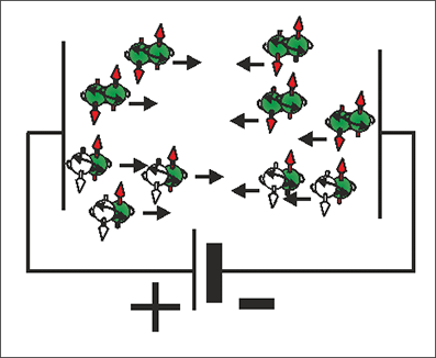
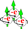
Spin and Charge TransportIn a solid all positively-charged particles (the protons) are localized inside an atomic nucleus and they do not transport the charge and the spin. Only negatively-charged particles (the electrons) transport the charge and the spin. However, some electrons with energies lower than the Fermi energy behave like positively-charged particles. For example, in an electrical field they diffuse from a "+" to a "-" drain. Therefore, the collective movement of negatively-charged electrons are described as a movement of positively- charged particles called the holes.
|
What do we know about holes in a solid? Is a hole a positive particle? Is there a real hole inside something? |
|
The holes in a solid are "spin" states with energy lower than the Fermi energy. They are negative particles with spin, but their behavior and properties are very similar to behavior and properties of a positive particle. There is no any real holes in the electron gas!!!! |
![]() What do we know about holes in a solid?
What do we know about holes in a solid?
![]() What do we know for sure:
What do we know for sure:
1. All positive particles are inside nucleus, they do not move inside a solid and their position in solid is fixed.
2. All charge and spin are transported by negatively-charged electrons.
3. Holes is a feature of electron gas, which makes electrons to behave like positive particles.
4. Holes are not unoccupied atomic orbitals. The transport of holes is not continuous jumping of electrons between neighbor atomic orbitals. A hole (electron) can not jump from an orbital to an orbital simply because the size of hole (electron) is substantially longer than the size of the orbital. For example in a semiconductor the size of a hole (the mean-free path) may exceed 1000-10 000 of atomic orbitals.
![]() Q. Are there real holes inside the electron gas?
Q. Are there real holes inside the electron gas?
No. There are only electrons in the electron gas. The electrons fills electrons states according to the Fermi-Dirac statistics. There are unfilled states, but they do not contribute to the transport.
There is a wrong view that a hole is unfilled atomic orbital and the electron from a neighbor orbital is scattered into this unfilled state. Therefore, the neighbor orbital becomes unfilled and the real hole literally moves from in the space. It makes the hole current. It is completely wrong view. If this were the case, the mobility of the hole would be extremely low. In contrast, the hole mobility is the same as the electron mobility in metals and it is only a little smaller than the electron mobility in the most of semiconductors. Even in some semiconductors (diamond, PbS, PbTe) the hole mobility is larger than the electron mobility .
The same as an electron current, the hole current is movement of electrons at a high speed in opposite directions. A little bit more electrons move in one direction than in another direction.
![]() Is any difference between holes in a semiconductors and holes in a metal? Are they of the same kind?
Is any difference between holes in a semiconductors and holes in a metal? Are they of the same kind?
Classical model consider a hole literally as a hole or a void in the ocean of electrons
|
| click on image to enlarge it |
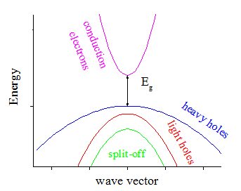
In a semiconductor, the electrons and the holes belong to different bands and have different symmetry. The electrons belongs to conduction band with s-symmetry and the holes belongs to the valence p-symmetry.
In a metal, there are near the same number of electrons and holes in each band. Often in a metal only one band crosses the Fermi energy and there are near-equal number of electrons and holes in this band.
In a semiconductor the hole and the electrons are easily distinguished, because they have different spacial symmetry:
The electrons have s-symmetry. They occupy the conduction band.
The hole have p-symmetry. They occupy the valence band.
In a metal in one band there are both the hole and the electrons. They have the same spacial symmetry, but they have different energy:
The energy of the electrons is above the Fermi energy.
The energy of the holes is below the Fermi energy.
 What is the hole? Is it a void in the ocean of electrons? Or it is an electron with special features?
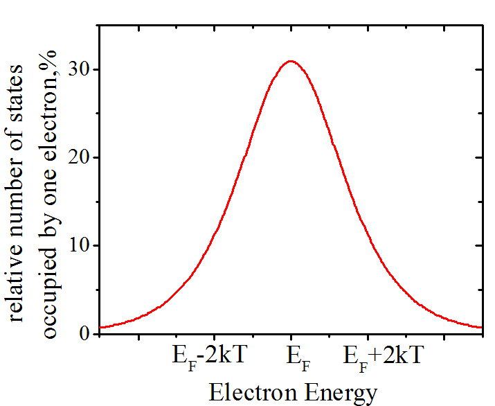
Fig.7 Number of quantum states occupied by one election (half-filled states) in a solid click on image to enlarge it |
|
Mainly the half-filled states participate in the charge, the spin and the heat transfer in a metal and a semiconductor. |
| Above the Fermi energy EF the slope is positive and the half-filled states are called the electrons |
| Below the Fermi energy EF the slope is negative and the half-filled states are called the holes |
| More details is here or |
| click on image to enlarge it |
.The holes are electrons, which energy is below the Fermi energy and which occupy quantum states, which is filled only by one electron.
Hole can be approximated as a void in the ocean of electron es in the case of electron energy substantially smaller than the Fermi energy. It is still relatively rough approximation.
In the vicinity of the Fermi energy there is no ocean of electrons and the void has no meaning at all.
![]() Q. A negatively-charged particle is attracted to "+" potential and it is repelled from "-" potential. If there are no any positively-charged particles in electron gas, how it is possible that in hole-type semiconductor the charge flows from "+" to "-"? Therefore, the transport particles are repelled from "+" potential and they are attracted to "-" potential?
Q. A negatively-charged particle is attracted to "+" potential and it is repelled from "-" potential. If there are no any positively-charged particles in electron gas, how it is possible that in hole-type semiconductor the charge flows from "+" to "-"? Therefore, the transport particles are repelled from "+" potential and they are attracted to "-" potential?
A .In electron gas the electrons do not simply follows the direction of an electrical field. The transport is more complex, which is explained as follows:
In a metal there are 1021 electrons per a cubic centimeter. It is a great number. It is about a billion times larger than the number of stars in our galaxy. In a semiconductor there are 1016 - 1019 electrons per a cubic centimeter.
All these electrons collide each other and move in all directions with a relatively high speed. Always the same amount of electrons move in any opposite directions.
An applied even-strong electric field does not change much. It does not reverse the movement direction of electrons. Still the electrons move in all directions. The speed of electrons does not change much as well. However, along the direction of electrical field there is a slight difference of number of electrons, which move in opposite directions. Even though this difference is a very tiny, it is sufficient to transfer the charge, the spin and the heat in the metal, because of the huge number of the conduction electrons.
The direction, in which a greater number of electrons move, depends on the energy distribution of electrons. The applied electrical field makes energy of electrons, which moves in the opposite directions, slightly different. A slope of energy distribution determines whether the number of electrons of a higher energy is larger or smaller. Therefore, it determines the direction of an average movement of electrons.
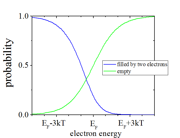
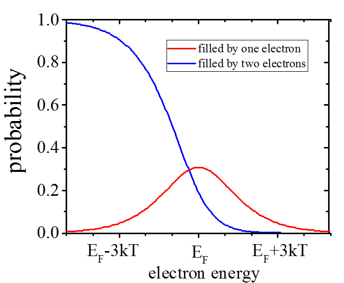
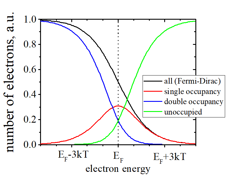
Figure 7 shows the energy distribution of quantum states in electron gas, which are occupied by only one electron (half-filled states). It has a maximum at the Fermi energy EF. It decreases for a higher energy, where all states are not occupied and it decreases for a lower energy, where all states are occupied by two electrons of opposite spins. Mainly the half-filled states participate in the charge, the spin and the heat transfer in a metal and a semiconductor.
As can be seen in Fig.7, in case of electron energy higher than the Fermi energy the slope of energy distribution is negative. It cause that the number of electrons, which move from "-" to "+", is greater than the number of electrons, which move from "+" to "-". Therefore, the average movement of the electrons is similar to a movent of negatively-charged particle, which all move in one direction along the electrical field from "-" to "+". Therefore, the electrons of energy higher than the Fermi energy are called the electrons.
In case of electron energy lower than the Fermi energy the slope of energy distribution is positive. It cause that the number of electrons, which move from "-" to "+", is smaller than the number of electrons, which move from "+" to "-". Therefore, the average movement of the electrons is similar to a movent of positively-charged particle, which all move in one direction along the electrical field from "+" to "-". Therefore, the electrons of energy lower than the Fermi energy are called the holes. (See Fig.8 below)
Classical model consider a hole literally as a hole or a void in the ocean of electrons
|
| click on image to enlarge it |
![]() Q. From the energy conservation law, only two possible charge movement directions are possible. Ether negatively- charged particles move from "-" to "+" or positively-charged particles move from "+" to "-". How it is possible that a negatively-charged electron moves from "+" to "-" ?
Q. From the energy conservation law, only two possible charge movement directions are possible. Ether negatively- charged particles move from "-" to "+" or positively-charged particles move from "+" to "-". How it is possible that a negatively-charged electron moves from "+" to "-" ?
In the case of holes the charge movement is in the correct direction. It is because along the movent of states, which are filled by one electron, there is a movement in opposite direction of states filled by two electrons. In total the negative charge of electrons moved from "-" to "+" as it should be.
However, most of the transport properties of the holes are determined by the half-filled states, but not full-filled states. For example, only the half-filled states may transport the spin. When a state is occupied by two electrons of opposite spins, the spin of the state is zero and such full-filled state can not transport the spin.
The contribution of the half-filled states to the ordinary Hall effect is substantially larger than the contribution of the full-filled states. It is because of a substantially different mean-free path for these two kinds of states.
![]() Q. In the case of holes, is it possible to use a positively-charged void in the see of electrons instead of the negatively-charged electrons in order to describe the hole transport?
Q. In the case of holes, is it possible to use a positively-charged void in the see of electrons instead of the negatively-charged electrons in order to describe the hole transport?
Yes, it is possible. However, it is only an approximation. In some cases this approximation can give an incorrect prediction.
It is better to verify the validity of this approximation for any particular cases.
The approximation of the positively- charged voids works well for electrons of an energy substantially lower than the Fermi energy.
Simple facts about holes in a metal and a semiconductor:
a quantum state filled by one electron. Q? Is it half-full? (it is the electron) or is it half-empty (it is the hole) A. It is both. At a higher energy the "spin" states is the electron and at a lower energy the "spin" states is the hole!!! |
Similar to a glass of wine, when a quantum state is filled only by one electron, it is called: - half-filled or the electron -half-empty or the hole.
|
|
 |
| The holes in a solid are "spin" states with energy lower than the Fermi energy. They are negative particles with spin, but their behavior and properties are very similar to behavior and properties of a positive particle. | click here or on image to enlarge it |
A semiconductor has two key properties, which a metal does not have.
Property 1: A semiconductor can be depleted. Therefore, a semiconductor can be switched from a conductor to an isolator.
Property 2: The electrons and the holes in a semiconductor belongs to different bands. It make the relaxation time between a hole and an electron to be relatively long about a few microseconds in a semiconductor. Since the relaxation between holes and electrons is slow, the electron and holes can coexist out from a common equilibrium for a long time. This property of a semiconductor makes possible the fabrication of a semiconductor laser and a bipolar transistor. Also, it makes possible existence of particles like an exciton.
In contrast, in a metal the relaxation time between a electron and a hole is very short about a few hundreds femtoseconds. The electrons and holes in a metal is always in a common equilibrium.
Note, the relaxation time is the average time during which a transition occurs of an electron from a quantum state in the conduction band into a quantum state in the valence band.
Each a quantum state for delocalized electrons (conduction electrons) may be filled maximum by two electrons of opposite spins. Main carriers of the charge, the spin and the heat are the quantum states, which are filled only by one electron. When the energy of these half-filled or half-empty quantum states is above the Fermi energy, these states are called the electrons. When their energy is below the Fermi energy, the quantum states of the conduction electrons are called the holes.
Does the hole have the spin? Is the spin of the hole different from the spin of the electron? |
|
yes, the hole has the spin. The spin of the hole is absolutely identical to the spin of the electron click on image to enlarge it |
Both the electron and the hole are a quantum state, which filled only by one electron (half-filled states). They are absolutely identical except their energy in the respect to the Fermi energy. Both the electron and the hole have the spin=1/2.
In a ferromagnetic metal, in which the electron gas is spin-polarized, the amount of the spin-polarized electrons and the spin-polarized electrons is nearly the same.
Under applied voltage the spin-polarized electrons and holes move in opposite directions. It explains the fact that the spin transfer by a drift current is very inefficient in bulk of a metal.
In the vicinity of interface the conductivities of holes and electrons become different, because of different mean-free paths. It makes the spin transport along an interface much more efficient.
In a metal with defects the mean-free path for the electron and the electron is different as well. Similar it makes the spin transport more efficient.
In a semiconductor the electrons and holes belong to different bands (the conduction band and the valence band). Therefore, they have different orbital moments. The electrons of the conduction band have none or very small orbital moment. The holes of valence band have a substantial orbital moment.
The spin may interact with orbital moment for both the conduction and localized electrons.
Depending whether the electron orbital moment is quenched or unquenched, the spin may interact or not with orbital moment.
The electrical field of a nucleus, the electrical field induced by charge accumulation or an external electrical field may induced substantial the spin-orbit interaction.
Both the hole and the electrons experience the spin-orbit interaction.
In a metal the electron and holes may have near the same magnitude, but opposite polarity of the spin-orbit interaction.
![]() (fact:) Both the "electrons" and "holes" are very similar particles, which are quantum states of an electron filled only by one electron. Each electron state can be filled maximum by two electrons of opposite spins. Only the difference between the "electrons" and "holes" is their energy with respect to the Fermi energy. How is that possible that such a small difference makes the "electrons" and "holes" of opposite charge.
(fact:) Both the "electrons" and "holes" are very similar particles, which are quantum states of an electron filled only by one electron. Each electron state can be filled maximum by two electrons of opposite spins. Only the difference between the "electrons" and "holes" is their energy with respect to the Fermi energy. How is that possible that such a small difference makes the "electrons" and "holes" of opposite charge.
![]() Are the holes really positively charged and the electrons negatively charged?
Are the holes really positively charged and the electrons negatively charged?
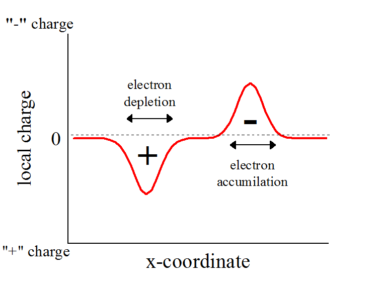
Fig. 33 Spacial charge distribution in a semiconductor and metals |
||||||
|
A. No. All conduction in a solid are negatively charged and only nuclei are positively charged. The electrons and holes are very similar. Both the electrons and holes are half-filled states, in which place is filled by an electron and another place is not filled. Only the difference between holes and electrons is that the energy of electrons is above the Fermi energy and the energy of holes is below the Fermi energy.
However, there is a charge accumulation associated with the electron and the charge depletion associated with the hole. Therefore, the electron can be associated with a negative charge and the hole can be associated with a positive charge.
Charge accumulation regions:
In a solid there is an equal number of negatively-charged electrons and positively charged protons. Therefore, the solid is not charged. Even locally, the charge distribution in a solid is very smooth and equals to zero everywhere (Fig. 33 left). A thermal fluctuation (a scattering) can move electron out from the equilibrium and the regions of charge accumulation and charge depletion are formed.
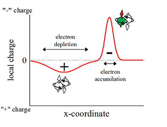
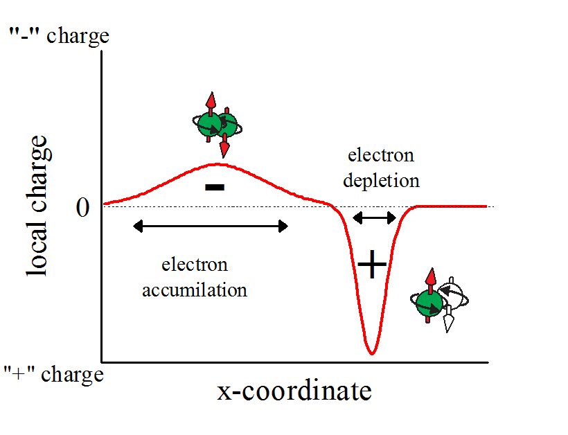
At an energy lower than the Fermi energy, the most of states are filled by two electrons of opposite spins. At an energy lower than the Fermi energy, the most of states are empty (See Fig.35). It causes different sign of charge accumulation region of the hole and electrons. At an energy lower than the Fermi energy, there is an electron depletion at place of the half-filled state (the hole) and there is an electron accumulation at place of the full-filled state. Therefore, the hole is positively charged (See Fig. 34 right). At an energy higher than the Fermi energy, there is an electron accumulation at place of the half-filled state (the electron) and there is an electron depletion at place of the empty state. Therefore, the electron is negatively charged (See Fig. 34 left).
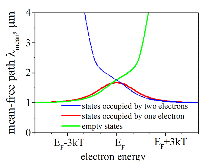
![]() Short effective length (the mean-free path) of a half-filled state makes region of charge accumulation/ depletion at place of the electron and the hole to be narrow and with high magnitude (spark-like).
Short effective length (the mean-free path) of a half-filled state makes region of charge accumulation/ depletion at place of the electron and the hole to be narrow and with high magnitude (spark-like).
The effective length or mean-free path is short for half-filled state and it is long for a full-filled state at an energy lower than EF and for an empty state at an energy higher than EF (See here). That makes narrow spark-like charge accumulation/ depletion region at place of the half-filled state and very broad region at place of full-filled state and empty state.
It is because of a different scattering probability for different state. In order to be scattered from a state the electron free space where to be scattered. For example, at energy sufficiently below the Fermi energy near all states are filled by two electrons of opposite spins (Fig.35). Therefore, near there is no any unoccupied state where an electron could scattered into. Therefore, in this case the life time of full-filled state is very long and the mean-free path is long as well. In contrast, an electron from a half-filled state can be scattered into empty state and a higher energy and an electron from full-filled state can be scattered into the half-filled state. Therefore, it is always many states are available for a scattering from/into a half-filled state. It makes the life time of half-filled state is short and the mean-free path is short as well.
| Fig. 34 Local charge of "Electrons" and "Holes". How "Electrons" and "Holes" become charged. | Fig.35 The distribution of full-filled and empty states | Fig.36. Mean-free path of states, which filled by two , one or none electrons | |||||||||||||||
|---|---|---|---|---|---|---|---|---|---|---|---|---|---|---|---|---|---|
|
|
|
|||||||||||||||
in both cases, the half-filled state becomes either a negatively-charged "electron" or positively-charged "hole", because of a smaller spatial size of the half-filled state in comparison of a larger- size "full-filled" state or "empty" state. Click on image to enlarge it. |
Click on image to enlarge it. | Click on image to enlarge it. |
A. No. Charge charge accumulation/ depletion region near each hole or electron can be distinguished only in a case when there are a few holes and electrons. For example in a semiconductor. When the density of holes and electrons become larger (for example, in a metal), the sum of all charged regions makes a very homogeneous and smooth charge distribution (Fig. 33 left) with any sparks.
A. Yes, in the case when there are positive and negative charge accumulation regions, they can attract each other. This can occur only in a semiconductor. See the question above.
In a semiconductor the Fermi energy EF is inside band gap. Therefore, electrons belong to conduction band of the s- symmetry and the holes belong to the valence band with the p- symmetry. Because of the different symmetry, the scattering probability of the electron into the hole is very low. The scattering time is about a few microseconds. The electron and the hole attract each other and stay at the same place for rather long time of about a microsecond. The properties of this pair of electron and holes slightly different for properties of individual holes and electrons. Therefore, this pair is considered as a new particle named exciton. The exciton life time is about a microsecond. After that time the electron is scattered into the hole forming a empty state in the conduction band and a full-filled state in the valence band.
A. No. In a metal the holes and the electrons belong to the same energy band. Therefore, they have the same symmetry. It makes the scattering probability between them very high. The average scattering time between electron and hole is about 10-100 femtoseconds. This time is too short to form an exciton. Another reason is that there is no spark charge accumulation region at place of hole or electron in metal.

Size of a "hole" |
 |
|
| Click on image to enlarge it |
The size of the "hole" is equal to the electron mean free path (see here) and it depends on the electron energy, the material quality and many other parameters.
The size of the "hole" can very from 1-10 nm in a metal to 10 -100 nm in a semiconductor. In some extreme cases at a low temperature , the size of a "hole" can exceed 1000 nm.
(note): Because of a smaller mobility, the size of the "hole" is smaller than the size of the "electron"
 vs
vs ![]() (fact) In order to confine both the "electrons" and "holes" inside a quantum well, the width of the quantum well should be smaller than the size of "electron" and the size of "hole"
(fact) In order to confine both the "electrons" and "holes" inside a quantum well, the width of the quantum well should be smaller than the size of "electron" and the size of "hole"
Since the size of a "hole" is usually smaller than the size of an "electron", the width of the Quantum Well should be smaller than the size of the "hole"
For most semiconductors, the width of a Quantum Well should not exceed 50 nm.
![]()
At a lower temperature, the size of a "hole" becomes larger. As a result, even a wider Quantum Well is able to confine a "hole"at a cryogenic temperature.
The energy level of dopants is close to the the Fermi level. Therefore, a dopant atom can catch or give an electron and the region of the charge accumulation/ depletion is created at place of the donor. The reciprocal region of opposite charge depletion/ accumulation is created at place of the hole or electron.
(quantum nature of electron) (restriction 1): The energy distribution of electrons is the Fermi- Dirac distribution.
(quantum nature of electron) (restriction 2): Each conduction electron occupies one quantum state. Each quantum state can be occupied by one or two conduction electrons
(quantum nature of electron)  (restriction 3): The electron can change its energy (e.g. in an electrical field) or movement direction only if the corresponded quantum state is unoccupied and available for the electron to be scattered into.
(quantum nature of electron) (restriction 4): The conduction electron can be scattered in a quantum state, which is already occupied by one electron, only when its spin is opposite to the spin of the already- existing electron
Energy distribution of electrons in a non-magnetic material, in which conduction electrons are not spin- polarized |
 |
(black line) Number of electrons vs. the electron energy. The Fermi- Dirac distribution. |
| (red line) Number of electrons in states, which are occupied by one electron |
| (blue line) Number of electrons in states, are occupied by two electrons of opposite spins |
| (black line)= (red line)+(blue line) |
| (red line) Number of of empty places in states, which is not occupied either by one or two electrons |
| Click on image to enlarge it |
(fact 1) ![]() The transport properties of a conduction electron are different whether it solely occupies a quantum state or together with another electron of opposite spin
The transport properties of a conduction electron are different whether it solely occupies a quantum state or together with another electron of opposite spin
(fact 2) ![]() The electron spin substantially influence the transport properties even in a non-magnetic metal, in which the electron gas is not spin polarized
The electron spin substantially influence the transport properties even in a non-magnetic metal, in which the electron gas is not spin polarized
The Current of hole is the current of electron with energy lower than the Fermi energy.
The half-filled states, which are filled by one electron, and full-filled states, which are filled by two electrons of opposite spins, contribute to the hole current.
The facts, which makes the hole current similar to the current of positively-charged particles.:
(1) Hall coefficient (Hall effect) is positive, but not negative as it should be for a current of negatively-charged particles.
(2) The spin is transferred by a drift current in direction from "+" to "-", but not from "-" to "+" as it should be for a current of negatively-charged particles.
 A: The half-filled states, which energy is below the Fermi energy, indeed move from "+" to "-" as a positively - charged particles. It explains all above features.
 (1) due to movement of an electron between scatterings.
It is most transport mechanism. It is major transport mechanism in bulk of metals and semiconductors.
I call this mechanism the current of the running-wave electrons.
(2) due to the scattering of electrons between quantum states.
It is substantially less efficient than previous mechanism.
It may become dominant mechanism for the transport in close vicinity of the interface, in a material with many defects or during a tunneling.
(Band Current): The band current is the major transport mechanism in the bulk of a conductor. It occurs due to movement of electrons between scatterings. Only the running-wave electrons contribute to this current.
Band CurrentSimple example |
||||||
|
![]() How the electrons transfer the charge and the spin in the band current?
How the electrons transfer the charge and the spin in the band current?
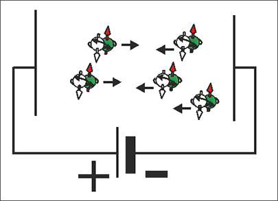
In a conductor the electron always move between scatterings. In an equilibrium equal amount of electrons move in any two opposite direction. Therefore in average there is no current. When voltage is applied, there are a little bit more electrons flows along voltage than in the opposite direction. Therefore, in average there is a current along the applied voltage.
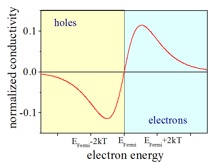
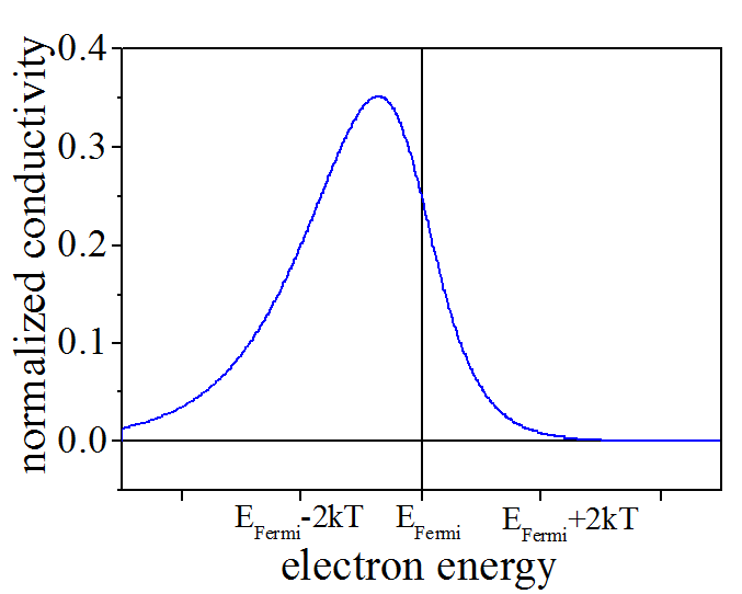
Why a negatively-charged electrons in the half-filled states move from "+" to "-" as positively -charged particles??The conductivity is linearly proportional to the derivative of the the distribution function. The distribution for half-filled states is peak-like (See Fig.7). For electrons with energy > EF , the derivative is negative. It means that in this case the states move as negatively-charged particles. However, for electrons with energy < EF (holes), the derivative is positive. It means that in this case the states move as positively-charged particles. The derivative of distribution of full-filled states is always negative. It means that in this case the full-filled states always move as negatively-charged particles(For more details See here).
The band current occurs because there is a difference of electrons, which moves in the opposite directions. For example, if an electrical field is applied between left and right. Then, in two neighbor regions the electrons at left will have a little higher energy than electron in the right region. Because of the energy distribution (the dependence of the number of electron on their energy), the number of electrons in the left and the right regions will be slightly different. Therefore, it will difference of the number of electrons, which move from left to right, and the number of electrons, which move from right to left. The band current will flow. The difference is linearly proportional to the derivative of the the distribution function.
|
|
||||||
Scattering of conduction electrons between different quantum states. The dark- yellow ellipse shows the electron wave functions. Each quantum state has two place for two electrons (spin- up and spin- down). The electrons (green balls) are frequently scattered between the quantum states. A scattering event occurs when (1) two quantum states are overlapped; (2) e.g. the wave functions of the electron and a defect are overlapped; (3) there is an unoccupied quantum state, in which the conduction electron can be scattered |
||||||
| click on image to enlarge it |
The conduction electrons contribute to the total conductivity unequally. The electrons of deep-energy levels nearly do not contribute at all. Only electrons with energy near the Fermi energy mainly conduct the spin and the charge in the electron gas.
Also, the conductivity is different for electrons occupying states, which filled by one electron and filled by two electrons of opposite spin.
Why?
Reason 1 (major) : The energy distribution of electrons occupying the half-filled and full-filled state are substantially different. (See above)
Reason 2 (minor): The mean-free path of electrons occupying the half-filled and full-filled state are substantially different. More details is here or![]() V Zayets,, arXiv(2014)
V Zayets,, arXiv(2014)
Why is an electron is faster and a hole is slower???
|
||
|
A simple answer would be
a) It is because the effective mass of electron is much smaller than the effective mass of an hole
b) It is feature of the band diagram
It does not explain any Physics. Both the electrons and the holes experience the same scatterings from the same defects. What is the difference between them?
My answer is
It depends on the material. In a metal, the mobility of electrons and holes is almost the same.
In a semiconductor, the electron mobility is larger than the hole mobility (except for a few exceptions)
The major reason of different motilities in a semiconductor is different special symmetry for electrons and holes.
The special symmetry of electrons is s- orbital like (spherical). The special symmetry of holes is p- orbital like.
It takes a longer time for an electron to circle the p- orbital than the s- orbital. It makes a hole slower than an electron.
(See here)
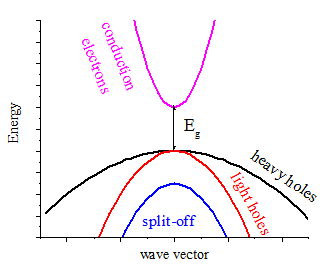
What is difference between a heavy hole and a light hole??? Their Weight?? |
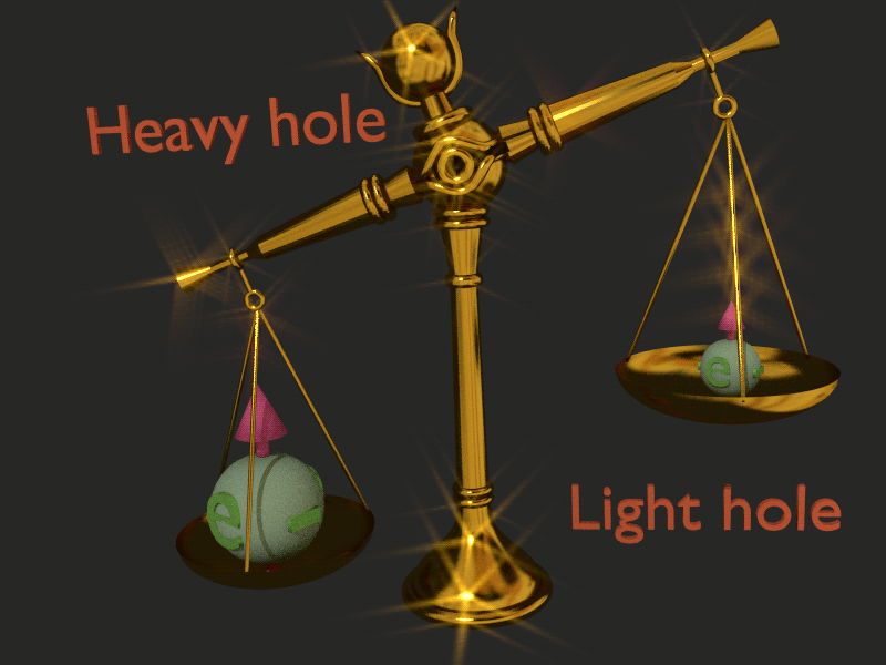 |
| The the light and heavy holes experience a different magnitude of the spin-orbit interaction, due to the different symmetry of their the spacial distribution. The spin-orbit interaction causes the difference of properties between the light and heavy holes. |
| click on image to enlarge it |
The electrons of the p- symmetry are divided into two classes: the light and heavy holes, because of the difference of their properties
The properties of the light and heavy holes are different, because of the difference of the spacial distribution of the light and heavy holes.
(reason of difference) ![]() The the light and heavy holes experience a different magnitude of the spin-orbit interaction, due to the different symmetry of their the spacial distribution. The spin-orbit interaction causes the difference of properties between the light and heavy holes. (details see here)
The the light and heavy holes experience a different magnitude of the spin-orbit interaction, due to the different symmetry of their the spacial distribution. The spin-orbit interaction causes the difference of properties between the light and heavy holes. (details see here)
The effective mass of heavy holes is usually larger than the mass of light holes.
(fact) ![]() The heavy and light holes are distinguished by their spin and orbital moment.
The heavy and light holes are distinguished by their spin and orbital moment.
(fact) ![]() In a metal, there are heavy holes, heavy electrons, light holes and light electrons
In a metal, there are heavy holes, heavy electrons, light holes and light electrons
spin is parallel to the orbital moment
J=3/2 (L=1 S=1/2) and J=-3/2 (L=-1 S=-1/2)
spin is antiparallel to the orbital moment
J=1/2 (L=1 S=-1/2) and J=-1/2 (L=-1 S=1/2)
(Note)![]() At gamma Γ point (the center of the Brillouin zone) in a zinc-blende semiconductor , the spacial orbital symmetry of the heavy and light holes are the same. As a result, their energies are the same.
At gamma Γ point (the center of the Brillouin zone) in a zinc-blende semiconductor , the spacial orbital symmetry of the heavy and light holes are the same. As a result, their energies are the same.
Orbitals of Heavy Holes Shape of orbitals depends on direction of the orbital moment. If orbital moment and spin is unquenched, the orbital shape depends on spin direction as well. |
||||
|
Direct-band semiconductor |
||||||
|
Both the standing-wave electrons and the running-wave electrons contribute to this current
The scattering current is the major transport mechanism in vicinity of a high-resistivity contact.
Electron scattering current |
Hole scattering current. |
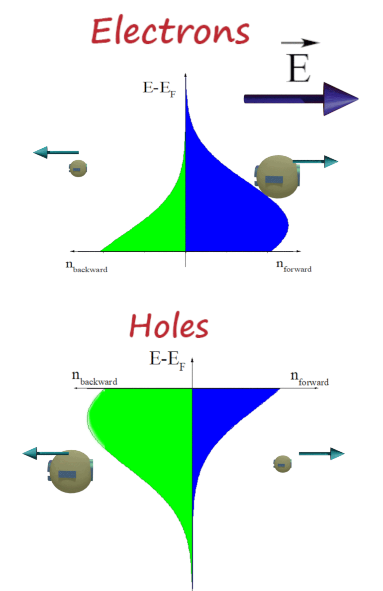
| Consequence scattering of an electron from a "spin" state into "empty" state corresponds to movement of "spin" states from right to left and to movement of "empty" from left to right . The spin and "-e" charge are transported in the same direction from the right to the left. | Consequence scattering of an electron from a "full" state into a "spin" state corresponds to movement of "spin" states from right to left and to movement of "full" from left to right. The spin and "-e" charge are transported in opposite directions. The spin is transported from the right to the left. The "-e" charge is transported from the right to the left. |
Scattering electron current |
Scattering hole current |
|
 |
| The scattering electron current in n-type semiconductor. The yellow cells indicates quantum states. In a n-type semiconductor the most states are "empty". There are a few half-filled states, which are filled only by one electron. Electrons are drifted through the sample by the scattering from a half-filled state into an "empty" state. At left side of the sample the directions of movement of half-filled and "empty" states are shown. At right side of the sample the directions of movement of a positive charge, a negative charge and spin are shown. Important: The spin moves from "-" to "+". It is opposite direction to the case of p- type semiconductor | The scattering hole current in p- type semiconductor. Spin-up current. The yellow cells indicates quantum states. In a p- type semiconductor the most states are filled by two electrons of opposite spins. There are a few half-filled states. Electrons are drifted through the sample by the scattering from a full-filled state into a half-filled state. At left side of the sample the directions of movement of half-filled and full-filled states are shown. At right side of the sample the directions of movement of a positive charge, a negative charge and spin are shown. Important: The spin moves from "+" to "-". It is opposite direction to the case of n-type semiconductor |
 |
|---|
click on image to enlarge it |
In a metal (also in a semiconductor) the electron and hole are the same object. They are both the negatively- charged electrons. The electrons and holes are distinguished by their energy with respect to the Fermi energy and more specific how their energy distribution (= number of electrons at at a specific energy) changes with an electron energy change. The energy of "electrons" is above Fermi energy and the energy of holes is below the Fermi energy. The number of "electrons" decrease when the electron energy increases. The number of "holes" decreases when the energy increases.
In a metal, the Fermi energy is inside of the electron band and therefore the number of electrons and the holes is nearly equal.
In a semiconductor, the Fermi energy is inside the band gap and there is a large difference in number of electrons above and below the Fermi energy. In a n- type semiconductor, the Fermi energy is just below the conduction band and there are many "electrons", but there are nearly no "holes". In a p- type semiconductor, the Fermi energy is just above the valence band and there are many "holes", but there are nearly no "electrons".
 Why the electron energy with respect to the Fermi energy defines whether an electron is the "electron" or the "hole"
One can distinguish between the "electron" and the "hole" by the direction, into which the electrons move in an electrical field. A negatively-charged particle moves from "-" to "+", but a positively-charged particle moves in the opposite direction from "+" to "-". Even though for both cases of the "electrons" and "holes", a single electron is always accelerated in an electrical field in the same direction from "-" to "+", this acceleration of a single electron courses different direction of the collective movement of the "electron" and "holes".
(where is the magic?) ![]() Why the same direction of movement of a single electron causes different direction of collective movement of many electrons?
Why the same direction of movement of a single electron causes different direction of collective movement of many electrons?
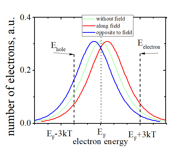
In a solid the conduction electrons move at a high speed in all directions even without an external electrical field. In absence of an external magnetic field, the numbers of electrons, which move in two opposite directions, are exactly equal. E.g. the number of conduction electrons, which move to the left, are the same as the number of the electrons, which move to the right. When an external electrical field is applied, for example, to the left direction, an electron, which moves along the field, accelerates and gains the energy. In contrast, an electron, which moves opposite to the electrical field, slows down and loses its energy. As a result, the electrical field makes an energy shift between the energy distributions for the electrons moving to the left and to the right and therefore the number of the electrons moving to the left and moving to the right, becomes different and therefore there is an electron current along the electrical field. The direction of the current is determined in which direction the left or the right there are more electrons moving.
| Numbers nforward and nbackward of forward- and backward- moving electrons vs. electron energy under an electrical field |
|---|
|
| Energy distribution of electrons under an electrical field. Right part (blue) shows electrons nforward moving along the electrical field (forward). Left part (green) shows electrons nbackward moving opposite to the electrical field (backward). The total number of electrons moving in each direction is calculated by an integration over all energies. |
| (note): The "electrons" are electrons, which energy is larger than the Fermi energy EF (shown in upper graph). The "holes" are electrons, which energy is smaller than the Fermi energy EF (shown in upper graph). |
| (note): The energy distributions of "electrons" and "holes" describes by the same distribution, the center of which is shifted under an electrical field. |
| (note): The An electron moving along electrical field gains the energy. In contrast, an electron moving opposite to electrical field loses the energy. As a result, the electron distribution of "electrons" and "holes" is shifted towards the electrical field. |
(electron current): More electrons move along the electrical field than opposite to the field (upper graph) |
(hole current): More electrons move opposite to the electrical field than along the field (upper graph) |
| click on image to enlarge it |
In the case of the "electrons" (the electrons, which energy are larger than the Fermi energy), the number of electrons decreases when the electron energy increases. It means that the number of the accelerated electrons, which moves to the left and gain the energy, becomes larger. In contrast, the number of the slowed electrons, which moves to the right and loss their energy, becomes smaller. This imbalance of the electron numbers results in the flow of the electron current to the left.
In the case of the "holes" (the electrons, which energy are smaller than the Fermi energy), the number of electrons increases when the electron energy increases. It means that the number of the accelerated electrons, which moves to the left and gain the energy, becomes smaller. In contrast, the number of the slowed electrons, which moves to the right and loss their energy, becomes smaller. This imbalance of the electron numbers results in the flow of the electron current to the right.
(it is the magic!!!) ![]() (Acceleration of a single electron along an electrical field causes the collective movement of electrons in the opposite direction)
(Acceleration of a single electron along an electrical field causes the collective movement of electrons in the opposite direction) ![]() As explained in above paragraph, the acceleration of electrons in one direction may decrease the decrease of the total number of the electrons, which is moving in this direction (the case of holes) and therefore create an electron current in the opposite direction. It happens due to frequent electron scatterings and redistribution of the electrons according the Fermi- Dirac energy distribution.
As explained in above paragraph, the acceleration of electrons in one direction may decrease the decrease of the total number of the electrons, which is moving in this direction (the case of holes) and therefore create an electron current in the opposite direction. It happens due to frequent electron scatterings and redistribution of the electrons according the Fermi- Dirac energy distribution.
(fact) ![]() The number of electrons, which participate in the electron transport, decreases when the electron energy becomes either larger or smaller than the Fermi energy (See here)
The number of electrons, which participate in the electron transport, decreases when the electron energy becomes either larger or smaller than the Fermi energy (See here)
(fact) ![]() The flow of the electron current in an electrical field occurs not because the electron move faster along the field, but because the number of electrons moving along the electric field becomes larger than the number of the electron moving opposite to the field.
The flow of the electron current in an electrical field occurs not because the electron move faster along the field, but because the number of electrons moving along the electric field becomes larger than the number of the electron moving opposite to the field.
![]() From Prameela: at some point in this discussion, it was asked about the higher values of electron mobilities. But there it was said that in metals, the mobilities of both electrons & holes is the same. Now my doubt is why will metals have holes at all. it would be only the electrons that are the charge carriers?
From Prameela: at some point in this discussion, it was asked about the higher values of electron mobilities. But there it was said that in metals, the mobilities of both electrons & holes is the same. Now my doubt is why will metals have holes at all. it would be only the electrons that are the charge carriers?
![]() A. Dear Prameela. A metal has nearly equal amounts of electrons and holes. In a metal, an electron and a hole are almost the same thing. The difference between them is only their energy with respect to the Fermi energy. In the vicinity of the Fermi energy the difference between an electron and a hole is negligible. We have learned from a semiconductor. The case of a semiconductor is special. In a semiconductor the Fermi level is in gap between two bands of very different symmetry. As a result, all electrons are of s- like symmetry and they belong to the conduction band. All holes are of p-like symmetry and they belong to the valence band. Because of the different symmetry, the scatterings between electrons and holes are rare and it is is possible to assign different quasi-Fermi levels for electrons and holes. This feature is determines all unique properties of the semiconductor. Because of different symmetry, many properties (like the mobility) is different for electrons and holes. The case of a metal is very different. The holes and electrons have the same symmetry and belong to the same band. Therefore, many of their property (e.g. the mobility) are the same. Still it is important to distinguish between holes and electrons in a metal. For example, the polarity of Hall effect is different in an electron-dominated metal and in a hole-dominated metal (See here). Even though, both the electron and the hole are in fact the electrons, in a solid they behave very differently. The electron behaves as a negatively-charged particle. The hole behaves as a positively -charged particle.
A. Dear Prameela. A metal has nearly equal amounts of electrons and holes. In a metal, an electron and a hole are almost the same thing. The difference between them is only their energy with respect to the Fermi energy. In the vicinity of the Fermi energy the difference between an electron and a hole is negligible. We have learned from a semiconductor. The case of a semiconductor is special. In a semiconductor the Fermi level is in gap between two bands of very different symmetry. As a result, all electrons are of s- like symmetry and they belong to the conduction band. All holes are of p-like symmetry and they belong to the valence band. Because of the different symmetry, the scatterings between electrons and holes are rare and it is is possible to assign different quasi-Fermi levels for electrons and holes. This feature is determines all unique properties of the semiconductor. Because of different symmetry, many properties (like the mobility) is different for electrons and holes. The case of a metal is very different. The holes and electrons have the same symmetry and belong to the same band. Therefore, many of their property (e.g. the mobility) are the same. Still it is important to distinguish between holes and electrons in a metal. For example, the polarity of Hall effect is different in an electron-dominated metal and in a hole-dominated metal (See here). Even though, both the electron and the hole are in fact the electrons, in a solid they behave very differently. The electron behaves as a negatively-charged particle. The hole behaves as a positively -charged particle.
![]() From Ken: Dear Sir, thank you for writing on this subject. It does not make sense to me and the explanations I have read on the Web dodge the real question. I would like to build on the question raised by Prameela, and add more details. (1) Please imagine a block of pure Silicon. The Silicon lattice locks the atoms in place and the atoms lock the electrons in place: the electrons therefore stay with their host atoms, bound by the positive charge of the nucleus. (As far as I know there are no free electrons moving around within the Silicon lattice.) Every atom in the block of Silicon has the same number of electrons and protons. Every Silicon atom in the block of Silicon is electrically neutral and the block itself is electrically neutral. There are no ions in the block. (1) Please imagine that this block is now doped with Boron atoms. In terms of electrical neutrality, nothing has changed. All Silicon atoms are neutral; all Boron atoms are neutral; the block itself is neutral. There are no ions in the block. (3) Magically a new entity appears in the block that wasn't there before. People call it a "hole" for no particular reason. The hole is not an atom, it is not an electron. I don't think it is any known subatomic particle. And magically these "holes' carry a positive charge. If you go back slightly in time, the Silicon atoms did not carry any electrical charge; the Boron atoms did not carry any electrical charge; the block of Silicon did not carry any electrical charge; nobody has connected the block of Silicon to a battery. Yet magically there are undefinable entities inside the block that carry positive charges that were not there before. And these undefinable entities move around within the Silicon lattice. People refer to this as P- Type Silicon. I believe the P stands for "positive." And within semiconductors the positive charge of these undefinable entities in the P- Type Silicon is said to attract free electrons from the N-Side. And when the N-Side free electrons diffuse over to the P- Type Silicon they are said to "fill the hole" or neutralize the positive charges that magically appeared in the P- Side. (4) My question is, where did a metal block containing Silicon atoms and Boron atoms that are 100% electrically neutral suddenly acquire positive electrical charges strong enough to attract free electrons from the N-Type Silicon and then neutralize free electrons that come within proximity?
From Ken: Dear Sir, thank you for writing on this subject. It does not make sense to me and the explanations I have read on the Web dodge the real question. I would like to build on the question raised by Prameela, and add more details. (1) Please imagine a block of pure Silicon. The Silicon lattice locks the atoms in place and the atoms lock the electrons in place: the electrons therefore stay with their host atoms, bound by the positive charge of the nucleus. (As far as I know there are no free electrons moving around within the Silicon lattice.) Every atom in the block of Silicon has the same number of electrons and protons. Every Silicon atom in the block of Silicon is electrically neutral and the block itself is electrically neutral. There are no ions in the block. (1) Please imagine that this block is now doped with Boron atoms. In terms of electrical neutrality, nothing has changed. All Silicon atoms are neutral; all Boron atoms are neutral; the block itself is neutral. There are no ions in the block. (3) Magically a new entity appears in the block that wasn't there before. People call it a "hole" for no particular reason. The hole is not an atom, it is not an electron. I don't think it is any known subatomic particle. And magically these "holes' carry a positive charge. If you go back slightly in time, the Silicon atoms did not carry any electrical charge; the Boron atoms did not carry any electrical charge; the block of Silicon did not carry any electrical charge; nobody has connected the block of Silicon to a battery. Yet magically there are undefinable entities inside the block that carry positive charges that were not there before. And these undefinable entities move around within the Silicon lattice. People refer to this as P- Type Silicon. I believe the P stands for "positive." And within semiconductors the positive charge of these undefinable entities in the P- Type Silicon is said to attract free electrons from the N-Side. And when the N-Side free electrons diffuse over to the P- Type Silicon they are said to "fill the hole" or neutralize the positive charges that magically appeared in the P- Side. (4) My question is, where did a metal block containing Silicon atoms and Boron atoms that are 100% electrically neutral suddenly acquire positive electrical charges strong enough to attract free electrons from the N-Type Silicon and then neutralize free electrons that come within proximity?
![]() A. I would like to answer your question step by steps. At first, I will clarify some details, which you have mentioned in your question. Next, I will answer to the main part of your question.
A. I would like to answer your question step by steps. At first, I will clarify some details, which you have mentioned in your question. Next, I will answer to the main part of your question.
(detail 1)![]() You wrote: : the electrons therefore stay with their host atoms, bound by the positive charge of the nucleus. (As far as I know there are no free electrons moving around within the Silicon lattice.)
You wrote: : the electrons therefore stay with their host atoms, bound by the positive charge of the nucleus. (As far as I know there are no free electrons moving around within the Silicon lattice.)
(localized and conduction electrons)![]()

![]() It is not correct. Only electrons of inner shells (like f- and d- electrons) stay with their host atoms (positive nucleus). Such electrons are called the localized electrons. The electrons of outer shells always move along the crystal lattice and do not stay at one host nucleus. In a solid, the atoms are very close to each other, the outer shells are strongly overlapped with neighbor shells forming the electron states covering all nucleuses. Such electrons are called conduction electrons. In a high- crystal -quality Si, the size (length) of conduction electron can be longer than one micrometer (See my Web page on the mean free path). It means that one conduction electron covers simultaneously more than a million of nucleuses. Also, simultaneously billions of conduction electrons overlap each other. All conduction electrons always move along the crystal lattice (even in equilibrium when there is no electrical current).
It is not correct. Only electrons of inner shells (like f- and d- electrons) stay with their host atoms (positive nucleus). Such electrons are called the localized electrons. The electrons of outer shells always move along the crystal lattice and do not stay at one host nucleus. In a solid, the atoms are very close to each other, the outer shells are strongly overlapped with neighbor shells forming the electron states covering all nucleuses. Such electrons are called conduction electrons. In a high- crystal -quality Si, the size (length) of conduction electron can be longer than one micrometer (See my Web page on the mean free path). It means that one conduction electron covers simultaneously more than a million of nucleuses. Also, simultaneously billions of conduction electrons overlap each other. All conduction electrons always move along the crystal lattice (even in equilibrium when there is no electrical current).
(reason why conduction electrons exists in a solid) ![]()
![]() It is easier to understand the fact of existence of the conduction electron in a solid by imagining an electron as a photon in a simplified 2D world. When an electron is confined in a single atom (e.g. in an atom of atomic gas), it is confined in a small area of atom. The confinement means that the electron bouncing back and forward between two imaginary mirrors or two walls. Because of the confinement (which is created by the electrical field of the nucleus), the electron cannot escape the atom. When many atoms are pushed together, the electron orbitals are overlapped, the confinement is broken (the walls are broken), there is no more back/forward reflection and the electron freely moves through all atoms.
It is easier to understand the fact of existence of the conduction electron in a solid by imagining an electron as a photon in a simplified 2D world. When an electron is confined in a single atom (e.g. in an atom of atomic gas), it is confined in a small area of atom. The confinement means that the electron bouncing back and forward between two imaginary mirrors or two walls. Because of the confinement (which is created by the electrical field of the nucleus), the electron cannot escape the atom. When many atoms are pushed together, the electron orbitals are overlapped, the confinement is broken (the walls are broken), there is no more back/forward reflection and the electron freely moves through all atoms.
(differences between localized and conduction electrons)![]()
![]()
![]() There are many substantial differences between conduction and localized electrons. (difference 1) A conduction electron overlaps millions of nucleus and millions of other conduction electrons. A localized electron is bound to one host nucleus and it only slightly overlaps its close neighbor localized electrons. (difference 2) Conduction electrons are scattered very frequently (~ each 500 fs). In contrast, a scattering of a localized electron is a rare event. (~ each ms or even a second). (difference 4) The conduction electrons are main contributors to the charge, spin, heat transport in a solid. The localized electrons have nearly no contribution to the transport. (difference 4) the distributions of spin directions are very different for localized and conduction electrons (See my Web page on spin polarization)
There are many substantial differences between conduction and localized electrons. (difference 1) A conduction electron overlaps millions of nucleus and millions of other conduction electrons. A localized electron is bound to one host nucleus and it only slightly overlaps its close neighbor localized electrons. (difference 2) Conduction electrons are scattered very frequently (~ each 500 fs). In contrast, a scattering of a localized electron is a rare event. (~ each ms or even a second). (difference 4) The conduction electrons are main contributors to the charge, spin, heat transport in a solid. The localized electrons have nearly no contribution to the transport. (difference 4) the distributions of spin directions are very different for localized and conduction electrons (See my Web page on spin polarization)
(transport mechanism by conduction electrons):![]()
![]()
![]() The transport mechanism of the conduction electrons is different from mechanism a water flow in river, but it is the same as the mechanism of wind flow in air. There are many conduction electrons and they all move in all different directions. In equilibrium, for any direction, the numbers of electrons moving in the forward and backward directions are precisely equal. Therefore, even though the conduction electrons are moving, in total as assembly they don't transfer the charge or the spin. When an electrical field or another distortion is applied, the subtle balance is broken and there are more condition electrons moving in one direction (e.g. along the electrical field) than in the opposite direction. As a result, the conduction electrons begin to transfer the charge and the spin. This is the general transport mechanism in a solid (See more detail here).
The transport mechanism of the conduction electrons is different from mechanism a water flow in river, but it is the same as the mechanism of wind flow in air. There are many conduction electrons and they all move in all different directions. In equilibrium, for any direction, the numbers of electrons moving in the forward and backward directions are precisely equal. Therefore, even though the conduction electrons are moving, in total as assembly they don't transfer the charge or the spin. When an electrical field or another distortion is applied, the subtle balance is broken and there are more condition electrons moving in one direction (e.g. along the electrical field) than in the opposite direction. As a result, the conduction electrons begin to transfer the charge and the spin. This is the general transport mechanism in a solid (See more detail here).
Electron current for "holes" and "electrons" |
||||||||||||||
|
||||||||||||||
|
||||||||||||||
| (electrons) |
||||||||||||||
| (holes) |
||||||||||||||
| Full description of the electron and hole current is here | ||||||||||||||
| click on image to enlarge it |
(in which material conduction electron exist) ![]()
![]() There are conduction electrons in any solid: in a metal, in a semiconductor and even in a dielectric. The transport properties of conduction electrons depend on availability of unoccupied states for conduction electrons (or the same: the number of states at the Fermi energy). As I described above, in order to transport the charge and/or the spin it should be more electrons moving in one direction than in the opposite direction. Therefore, some unoccupied state should be available for conduction electrons moving in the forward direction. In a metal, there are plenty of unoccupied states and therefore the metal is a good conductor. In contrast, in a dielectric there is no any unoccupied state. Since all states are occupied, the electrons cannot be scattered from a state or into a state and therefore the number of moving in any specific direction cannot be changed. As a result, the conduction electrons cannot transport any charge or spin in a dielectric. It is the fact that there are lots of conduction electrons in a dielectric, all conduction electrons move in all directions, but they cannot transport any charge or spin. The existence of conduction electron in a dielectric is experimentally well- verified fact. For example, the light absorption and refractive index in the dielectric is purely determined by the conduction electrons for a short wavelengths when a photon energy is larger than the dielectric band gap.
There are conduction electrons in any solid: in a metal, in a semiconductor and even in a dielectric. The transport properties of conduction electrons depend on availability of unoccupied states for conduction electrons (or the same: the number of states at the Fermi energy). As I described above, in order to transport the charge and/or the spin it should be more electrons moving in one direction than in the opposite direction. Therefore, some unoccupied state should be available for conduction electrons moving in the forward direction. In a metal, there are plenty of unoccupied states and therefore the metal is a good conductor. In contrast, in a dielectric there is no any unoccupied state. Since all states are occupied, the electrons cannot be scattered from a state or into a state and therefore the number of moving in any specific direction cannot be changed. As a result, the conduction electrons cannot transport any charge or spin in a dielectric. It is the fact that there are lots of conduction electrons in a dielectric, all conduction electrons move in all directions, but they cannot transport any charge or spin. The existence of conduction electron in a dielectric is experimentally well- verified fact. For example, the light absorption and refractive index in the dielectric is purely determined by the conduction electrons for a short wavelengths when a photon energy is larger than the dielectric band gap.
(detail 2) ![]() You wrote: The hole is not an atom, it is not an electron.
You wrote: The hole is not an atom, it is not an electron.
The hole is the electron. The is not an atom, or a nucleus, or any type of a positively- charged particle or any kind of a void. The hole is a negatively- charged electron, which at condition in a solid behaves exactly as a positively- charged particle. A good example is a metal, in which the electrons of an energy higher than the Fermi energy are "electrons" and the electrons of an energy lower than the Fermi energy are "holes".
(the reason why the electron behaves as a positively-charged particle and why the Fermi energy is matter) ![]()
![]()
![]() As I explained above, an electron current flows when there are more electrons moving in the current direction than in the opposite direction. When the electrical field is applied, an electrons, which move along field, accelerate and gain energy. In contrast, the electrons, which move in the opposite direction, slow down and loss energy. The change of the electron energy changes the number of electrons moving in each direction. The dependence of the number of electrons on an electron energy is called the electron energy distribution (See here). As a result of applying of the electrical field, the energy distribution of electrons moving along the field shifts up and the energy distribution of electrons moving opposite to the field shifts down. It
As I explained above, an electron current flows when there are more electrons moving in the current direction than in the opposite direction. When the electrical field is applied, an electrons, which move along field, accelerate and gain energy. In contrast, the electrons, which move in the opposite direction, slow down and loss energy. The change of the electron energy changes the number of electrons moving in each direction. The dependence of the number of electrons on an electron energy is called the electron energy distribution (See here). As a result of applying of the electrical field, the energy distribution of electrons moving along the field shifts up and the energy distribution of electrons moving opposite to the field shifts down. It
(detail 3) ![]() You wrote: If you go back slightly in time, the Silicon atoms did not carry any electrical charge; the Boron atoms did not carry any electrical charge; the block of Silicon did not carry any electrical charge; nobody has connected the block of Silicon to a battery. Yet magically there are undefinable entities inside the block that carry positive charges that were not there before.
You wrote: If you go back slightly in time, the Silicon atoms did not carry any electrical charge; the Boron atoms did not carry any electrical charge; the block of Silicon did not carry any electrical charge; nobody has connected the block of Silicon to a battery. Yet magically there are undefinable entities inside the block that carry positive charges that were not there before.
(charge of doped silicon): Each the semi insulating (undoped) silicon, p-Si (e.g. silicon doped with boron) and n-Si (e.g. silicon doped with phosphorous) is absolutely uncharged. The total positive charge of all nucleases precisely equal to the total negative charge of all electrons.
(reason why undoped silicon is not conductive): The undoped silicon (i-Si) has a lot of conduction electrons, but there is no unoccupied state, the conduction electrons occupied all available quantum states and therefore the conduction electrons are unable to transport the Charge or the Spin. There is an energy band to the close unoccupied states and the conduction electrons cannot be scattered to those states. As I have explains above, in order to transport the Charge and the Spin, the conduction electrons should be able to change their direction distribution. In one direction it should be more electrons and in the opposite direction should be less. In the absence of unoccupied states the conduction electrons are unable to do that and therefore unable to do any transport. This reason id the same to the reason why the conduction electrons cannot make any current in a dielectric.
(reason why silicon doped with phosphorous becomes conductive): An atom of phosphorous has one more electron on outer shell than an atom of the Si and therefore one more of its electrons become a conduction electron . As a result of replacing a few of atoms of Si by atoms of phosphorous in the crystal of Si, the number of conduction electrons in Si slightly increases and the subtle balance between equal number of conduction electrons and their quantum states is broken. Since there are no available unoccupied states, these additional conduction electrons occupies the upper states (conduction band) of a higher energy, there is a huge number of unoccupied quantum states there. Therefore, these additional conduction electrons, which are provided by the phosphorous, are able to transport the Charge and the Spin.
(reason why silicon doped with boron becomes conductive): An atom of boron has a smaller number of electrons on outer shell than an atom of the Si and therefore less of its electrons become the conductive electrons. As a result of replacing a few of atoms of Si by atoms of boron in the crystal of Si, the number of conduction electrons in Si slightly decreases and the subtle balance between equal number of conduction electrons and their quantum states is broken. There are more available quantum states than the conduction electrons and some of quantum states become unoccupied. Since there are unoccupied states, the conduction electrons are are able to transport the Charge and the Spin. This main band is called the valence band and the unoccupied quantum states are called the holes.
(charged pn junction) At a contact of a p-Si and n-Si, some conduction electrons from n-Si move into p-Si and some non-conductive region is formed, in which the balance between the number of conduction electrons and quantum state become equal again. As a result, a tiny region at contact in the p-Si becomes negatively- charged and a tiny region in n- Si becomes positively- charged.
Abhishek Chauhan · Shri Mata Vaishno Devi University
![]() Electrons travel in the conduction band between the two materials. Since the conduction band is formed by the uppermost shell, farthest from any of the nucleus, and since proton resides inside nucleus and hence more energy is required to move an proton than an electron
Electrons travel in the conduction band between the two materials. Since the conduction band is formed by the uppermost shell, farthest from any of the nucleus, and since proton resides inside nucleus and hence more energy is required to move an proton than an electron
Joel T. Asubar · 20.37 · 25.34 · Hokkaido University
![]() Holes are absence of electrons in covalent bond and hole movements are actually movement of electrons to fill up an adjacent hole in the covalent bond. Thus, the electrons moving this way are still under the influence of nucleus forces that scatter them. In contrast, free electrons (or just commonly referred to as electrons) move within the semiconductor material freely, without going from a covalent bond vacancy to another. Meaning, free electrons are less influenced by the scattering due to nucleus forces and hence the higher mobility.
Holes are absence of electrons in covalent bond and hole movements are actually movement of electrons to fill up an adjacent hole in the covalent bond. Thus, the electrons moving this way are still under the influence of nucleus forces that scatter them. In contrast, free electrons (or just commonly referred to as electrons) move within the semiconductor material freely, without going from a covalent bond vacancy to another. Meaning, free electrons are less influenced by the scattering due to nucleus forces and hence the higher mobility.
![]() my comment:
my comment:
Explanation given by Joel T. Asubar is not correct.
The movement of holes is not movement of electrons to fill up an adjacent hole in the covalent bond. The movement of a hole is as "free" as the movement of an electron. In fact, both the electrons and the holes are the same delocalized electrons. For example, in a metal the electrons and holes can be only distinguished by their energy. The energy of an electron is above the Fermi energy and the energy of a hole is below the Fermi energy. Of cause, an electron and a hole interact differently with electrical field.
The mean-free path of a hole may reach several micrometers (typically in a semiconductor it is 50-200 nm at room temperature). If you see an electron as a wave, the mean-free path of an electron is just the size of the electron. Therefore, the size of a hole may be a micrometer. The distance between covalent bonds is about 0.1 nm. It means that simultaneously an electron or a hole is filling up or interacts with a million of covalent bonds. Surely, the movement of holes is not movement of an electron to fill up adjacent holes in the covalent bonds. Besides, in order to jump from one covalent bond to other covalent bond an electron needs to interact with a phonon. In the case if such jumping between the covalent bonds were the mechanism of the hole transport, the hole mobility would be very small. It would be even smaller than mobility in a material with hopping conduction.
In a metal the electron mobility and the hole mobility is the same. Only reason for a difference in the mobilities in a semiconductor is different spatial symmetry of the envelop function for an electron and a hole.
![]() following question
following question
Thank you Vadym Zayets for the detailed explanation considering spin-orbit interaction. However, I have a little doubt in my mind. As you pointed out, both are delocalized electrons having only difference in spatial symmetry,how would you explain the effective mass of electrons is smaller than hole in accordance with your explanation?
my answer
The mobility of electrons and holes is different, because the electrons and holes have different spatial symmetry. The electrons have s-orbital -like symmetry of the envelop wave function. The holes have p-orbital -like symmetry of the envelop wave function.
There are two reasons why the difference in the spatial symmetry causes the different mobility. They may sound different, but they explain the same fact.
The first reason, why the mobility is different, is that it takes a longer time for an electron to circle around the p-orbital than around the s-orbital.
A delocalized electron simultaneously moves along the crystal lattice and rotates around millions of atomic nuclei . It might sound strange that it is possible to rotate around several objects simultaneously. Since an electron is a wave, it is possible. For example, when light is diffracted by a diffraction grating , each photon is reflected from each of million steps of the grating) simultaneously. Any wave can interact with many objects simultaneously. It is not forbidden.
There are many experimental proofs that delocalized electrons have a non-zero orbital moment. For example, their g-factor is different from 2, they experience the center-symmetrical spin-orbit interaction and the existence of the split-off valence band is other proof. The non-zero orbital moment literally means that the delocalized electron is orbiting around atomic nuclei.
The second reason, why the mobilities (effective masses) are different for holes and electrons in a semiconductor, is that the magnitudes of the s-like and p-like envelope functions are different in the vicinity of the atomic nucleus. The electrons of different symmetry interact differently with the nucleus. Therefore, the amplitude of the lattice periodic potential is different for electrons and holes in a semiconductor. This causes the different effective masses.
Mobility is proportional to the average time between two consecutive scattering events (collisions) and is inversely proportional to the effective mass. Electrons and holes are scattered by different types of crystal imperfections, which include phonons, impurities, defects, etc. In current MOSFET transistor, the channel electrons and holes are scattered mainly by impurity and interface charges (Coulomb scattering), interface roughness, and phonons. The average time between collisions (also known as the mean free time) is given by the Mathiessen's Rule. For most semiconductors (elemental, III-V compounds, II-VI compounds, etc.), the electron mobility is larger than the hole mobility, and in some cases much larger; but there are exceptions. Exceptions are: electron mobility/hole mobility in cm-2V-1s-1: C (Diamond) - 1800-2200/1600-1800; PbS - 600/700; PbTe - 2500-6000/1000-4000.
I have a question that mobility of holes in oxides having 2p orbital (e.g. gallium oxide) is less compared to mobility of holes in oxides having 3d orbital, e.g. copper oxide , why this is so? I have followed your answers on difference in mobility of electrons and holes but still didn't get answer to this question. Could you please explain it to me.
![]() Firstly, the mobility does not depend whether the electron is the “electron” or “hole”. For example, the mobility of the holes and electrons in a metal is absolutely identical. Whether it is a hole and an electron are only distinguished by the electron energy in respect to the Fermi energy. The energy of a hole is smaller than the Fermi energy, the energy of an electron is greater. Generally the energy of an electron of p-symmetry is smaller than an electron of s-symmetry and the energy of an electron of d-symmetry is smaller than an electron of p-symmetry as it follows the electron arrangement in a free atom (it is not always the case). Therefore, an electron of p- or d-symmetry is often the hole, but an electron of p- or d-symmetry is often the “electron”.
Firstly, the mobility does not depend whether the electron is the “electron” or “hole”. For example, the mobility of the holes and electrons in a metal is absolutely identical. Whether it is a hole and an electron are only distinguished by the electron energy in respect to the Fermi energy. The energy of a hole is smaller than the Fermi energy, the energy of an electron is greater. Generally the energy of an electron of p-symmetry is smaller than an electron of s-symmetry and the energy of an electron of d-symmetry is smaller than an electron of p-symmetry as it follows the electron arrangement in a free atom (it is not always the case). Therefore, an electron of p- or d-symmetry is often the hole, but an electron of p- or d-symmetry is often the “electron”.
You can look in more details about this topic in the following my paper
V. Zayets, ", JMM 445, pp 53–65 (2018).
You can download it here
Secondly, the mobility of the electron depends more on crystal symmetry than atomic symmetry (s-,p-,d-). For example, it is believed that d-electrons in Fe metal are localized for e_1g symmetry and delocalized for t_2g symmetry. Therefore, the d-electrons in iron have zero mobility, when they have e_1g symmetry, and they have reasonably high mobility, when they have t_2g symmetry.
You can understand it as follows.
The mobility of an electron depends on the length of the electron. The longer length of the electron, the greater its mobility. (of course, the mobility is also depends on several other parameters)
The length of an electron depends how well the electron function of neighbor atoms are overlap. Within oversimplify view, more they overlap, longer the electron length is.
 I do not now details about band structure of gallium oxide and copper oxide.
A possible explanations is as follows.
The oxide are mainly ionic crystals. The oxygen takes one or two s- or p- from Ga ore Cu. Therefore, s- or p- electrons becomes localized and they do not participate in the conductivity. In contrary, d- or p- electrons are still near its host atom, their neighbor-atom wave functions can overlap and they become delocalized conduction electrons. Of course, everything depends on crystal symmetry. Additionally, the wavefunction could be elongated due the Coulomb's repulsion from neighbor oxygen.
Everything depends on crystal symmetry and atom arrangement. An electron of d-symmetry may have greater mobility that an electron of p-symmetry.
![]() Question from Szymon Królak
Question from Szymon Królak
I would like to thank you for your in-depth analysis of the electron-hole concept. To see that someone speaks about holes as electrons (which they are) and not some positive charge was a great relief. I have a question regarding the Hall effect in a p-type semiconductor. On your page, you explain it using holes as carriers of the positive charge. How is that? I thought, based on your explanation, that holes possess a negative charge.
I would like to thank you for your in-depth analysis of the electron-hole concept. To see that someone speaks about holes as electrons (which they are) and not some positive charge was a great relief. I have a question concerning Fig. 15. I understand, why holes, bearing negative charge are on the right side of a p-type block. Why are full-filled states displaced to the left? Is it because they also have negative effective mass (as the half-filled states)?
 (answer)
The full state or a state filled by two electrons of opposite spin has a negative slope of the distribution function. This is the same polarity of the slope as that for the "electrons”, but opposite to that of "holes". In fact, the energy distribution is a property of many electrons. It describes how many electrons have a specific energy. The slope defines whether the number of electrons decreases or increases for a different energy of electrons. The electron distribution is defined by the electron scatterings and the spin properties. Just a brief explanation of the important points
(point 1):
Both the electrons and holes are electrons.
Both "electron" electron and "hole" electron are accelerated in an electrical field in the same direction from "-" to "+".
(point 2):
Even in the absence of an electrical field, all electrons are moving at a substantial speed.
However, the number of electrons, which move in any direction, is exactly equal to the number of electrons, which move in the opposite direction.
As a result, on average there is no charge transfer.
(point 3)
In an electrical field, both the "electron" electron and the "hole" electron are accelerated from "-" potential to "+" potential.
The electrons, which move along the electrical field, accelerate and gain their energy.
The electrons, which move opposite to the electrical field, are slowing down and losing their energy.
As a result, the average energy of electrons, which move along the electrical field, is larger than the average energy of electrons, which move opposite to the electrical field.
Therefore, the energy distributions of opposite-moving electrons are shifted with respect to each other and, as a result, the number of the electrons moving to the forward direction becomes different from the number of the electrons moving in the opposite direction and, on average, there is an electrical current.
(point 4)
In the case of "electron" electron, the slope of the energy distribution is negative.
It means that when the energy distribution is shifted to the higher energy, the number of the electrons increases
It means that in the case of "electron" electrons, the number of electrons moving along the electrical field is larger than the number of the electrons moving in the opposite direction and , on average, the electron current flows along the electrical field.
In the case of "hole" electrons, the slope of the energy distribution is positive. It means that when the energy distribution is shifted to the higher energy, the number of the electrons decreases
It means that in the case of "hole" electrons, the number of electrons moving along the electrical field is smaller than the number of the electrons moving tin the opposite direction and , in average, the electron current flows opposite to the electrical field as if it is a current of a positive particles
(point 5)
The spin plays an important role in the electron transport even in a non-magnetic material, which has no magnetic properties at all.
Each electron quantum state can be filled either by zero electrons (an empty state) or by one electron (a spin state) or by two electrons of opposite spin (a full state).
At a very low energy, all quantum states are filled. Therefore, all states are full.
At a very high energy, there are no electrons. Therefore, all states are empty.
As a result, the number of the full states monotonically decreases from a larger number (all states are full states) to zero (there is no full state) as the electron energy increases. The slope of the energy distribution of full states is always negative.
The number of the empty states monotonically increases from zero (there is no full state) to a larger number (all states are full states) as the electron energy increases. The slope of the energy distribution of empty states is always positive.
The number of the spin states at first increases from zero (there is no spin state at a very low energy) to some number, next decreases to zero (there is no spin state at a very high energy). As a result, at first the slope of the energy distribution of spin states is positive, next it changes to negative. The change of the slope polarity occurs at the Fermi energy.
Therefore, the electrons of the spin states moves opposite to the electrical field, when their energy is lower than the Fermi energy ("holes") , and moves along the electrical field, when their energy is higher than the Fermi energy ("electrons")
The negatively-charged electrons, whose energy is below the Fermi energy, collectively behave as positive particles, even though each electron behaves as a negative particle.
(point 6)
There are two different electron currents: 1: current of the spin states and 2: current of the full states.
Even in the case of electron energy below the Fermi level (holes), on average over these two currents, more electrons flow from "-" to "+" than in the opposite direction. Therefore, there is no breaking of the fundamental Law for the charge here.
However, since the slope of the distribution of the spin states is substantially larger than that of the full states, the most of the transport effects (like the Hall effect) is defined mostly by the current of the spin states, which is the same as a current of positive particles.
(point 7) semiconductor
In a semiconductor, the Fermi level is in the gap between two electron bands of a very different symmetry (the conduction band and the valence band).
The probability of the electron scattering is very low between electrons of these two states. As a result, two individual Fermi levels for conduction and valence electrons may exist in a non-equilibrium state e.g. in the case of the electron transport.
Many semiconductor transport effects (e.g. a bipolar transistor or a semiconductor laser) are based on this symmetry difference, but not on a difference between the electron and hole transports.
For example, a metal has about equal number of electrons and holes at same time. However, both the hole and electrons belong to the same band and, therefore, the electrons and holes have the same symmetry. Because of the same symmetry, even though there are many electrons and holes in a metal, it is impossible to make a bipolar transistor or a laser diode using a metal and the hole- electron recombination as it is made in a semiconductor.
(point 8) The positively-charged particles for "holes"
It is possible and helpful to introduce positive particles for the hole current as empty or unfilled states.
Similar as an electron can be either in a full state (the state filled by two electrons) or in a spin state (the state filled by one electron and having one unfilled electron place), the unfilled electron place can be in the spin state or in the empty state (both electron places are unfilled)
In absence of an electrical field, the number of unfilled electron places is the same in all directions.
Under an electrical field, the distribution of unfilled electron places becomes different in the direction along the filled and the direction t opposite to the field. As a result, there is a current of these unfilled electron places from "+" to "-" potential. It is similar as if there is a flow of positively-charged particles.
This representation is useful for processes, which are based on an electron scattering between a filled state of the conduction band and an unfilled state of the valence band. Examples of a process are a bipolar transistor and a semiconductor laser.
Still it is important to remember that it is the electrons, which are scattered, transfer the charge and the spin and, therefore, define all transport properties.
response from Szymon Królak
thank you for this exhaustive explanation. Somehow, I missed point 3. Now I understand, that even though the "holes" and "electrons" are accelerated in the same direction by the electrical field, their respective currents are in the opposite directions, because of the slope of the distribution function. Also, now I see how important it is to operate with statistical measures concerning the electrons in a solid, just like you said: "The negatively-charged electrons, which energy is below the Fermi energy, collectively behave as positive particles, even though each electron behaves as a negative particle".
I will try to answer your questions as soon as possible