Dr. Vadym Zayets
v.zayets(at)gmail.com
My Research and Inventions
click here to see all content |

Dr. Vadym Zayetsv.zayets(at)gmail.com |
|
|
more Chapters on this topic:IntroductionTransport Eqs.Spin Proximity/ Spin InjectionSpin DetectionBoltzmann Eqs.Band currentScattering currentMean-free pathCurrent near InterfaceOrdinary Hall effectAnomalous Hall effect, AMR effectSpin-Orbit interactionSpin Hall effectNon-local Spin DetectionLandau -Lifshitz equationExchange interactionsp-d exchange interactionCoercive fieldPerpendicular magnetic anisotropy (PMA)Voltage- controlled magnetism (VCMA effect)All-metal transistorSpin-orbit torque (SO torque)What is a hole?spin polarizationCharge accumulationMgO-based MTJMagneto-opticsSpin vs Orbital momentWhat is the Spin?model comparisonQuestions & AnswersEB nanotechnologyReticle 11
|
Technology of nano contact How to make small features by electron-beam (EB) lithography Technology
Even though by electron-beam (EB) lithography it is relatively easy to make features larger then hundred nanometers the following tips might be useful the larger features as well.. How to make devices with features smaller than 100 nm by EB lithography. Tips:1) Use chemically-amplified relatively-thick EB resists (thickness 150-300 nm).2) Use the modulated exposure. Borders of your features should be exposed more then the middle.3) A good focusing of EB beam is important.4) For example, in order to a fabricate nanomagnet with diameter of 30 nm, it is better not to draw a nano dot of 30-nm diameter. Instead it is better to draw a larger nano dot with diameter of 100 nm with optimized border profile. Next, the diameter should be reduced by the slimming.5) Use enhancement of surface adhesion.6) Move your sample very gently in developer and water.7) Do not rinse (keep) your sample in water longer than 10-20 sec. The small features of EB resist may be deformed in water.8) Smallest feature should be across movent of EB beam. For example, usually the EB beam moves from left to right (along the x-axis). Than, long axis of ellipse should be along x-axis and short axis should be along y-axis.Modulated -exposure method
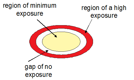
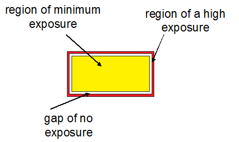
By this method the shape of the etched EB resist is controlled. (See Fig 3 below) Idea: Instead of homogeneous EB exposure of an area of an object, the exposure area is divided into 3 areas: 1) border area of a high and optimized exposure 2) gap of no exposure 3) main area of a minimum-possible exposure The widths of the border area and the gap should be optimize according to the sensitivity and thickness of EB resist and the maximum e-beam modulation speed of your EB machine. ----------------------------- Obstacle for EB lithography: Electron proximity effect When the electron beam exposes a desired area of EB resist, the electrons are reflected from the sample at different angles and some undesirable area becomes exposed as well. In order to reduce undesirable consequences of the electron proximity effect, the smallest possible exposure should be used. In this the number of reflected electron is not sufficient to expose the EB resist in undesirable areas. However, weakly-exposed EB resist can not keep well its shape. Therefore, higher exposure is necessary at the edge of writing shape. Another merit of the modulated -exposure method is that edge of the EB resist can be optimized. .j01 files of different shapes for modulated-exposure method can be found at bottom of this page . Isolation layerIt is used for an electrical isolation between a back and top electrodes of a nonocontact. The deposition of the isolation layer is followed by the lift-off or planarization process, which both are very sensitive to the thickness of the isolation layer.
|
EB exposure of a large-size object by modulated -exposure method see examples in different shapes.zip |
 |
2) Al2O3 is amorphous. The 15 -30 nm of Al2O3 provides a good isolation. Major problem: Al2O3 is etched by resist developer. It makes a lot of headache for the following fabrication processes.
3) Ti2O3 is amorphous. The 15 -30 nm of Ti2O3 provides a good isolation. Major problem: during sputtering the Ti2O3 tends to crystallize into small particles inside the chamber. It makes the sputtering chamber dirty in a short time.
After deposition of the isolation layer the EB resist of nano contact is covered by the isolation material. In order to open the nano contact either the lift-off or the planarization is used.
The planarization is more useful for larger-size samples. It is often used for mass production in companies.
The lift-off is more useful for smaller-size samples. It is often used in institutes and universities.
Method 1: Mechanical polishing.
The height of area with EB resist is higher than in area with EB resist. The mechanical polishing removes the isolation material in areas with EB resist and it does not damage the isolation in areas without EB resist.
Method 2: RIE etching (a wet etching might work as well)
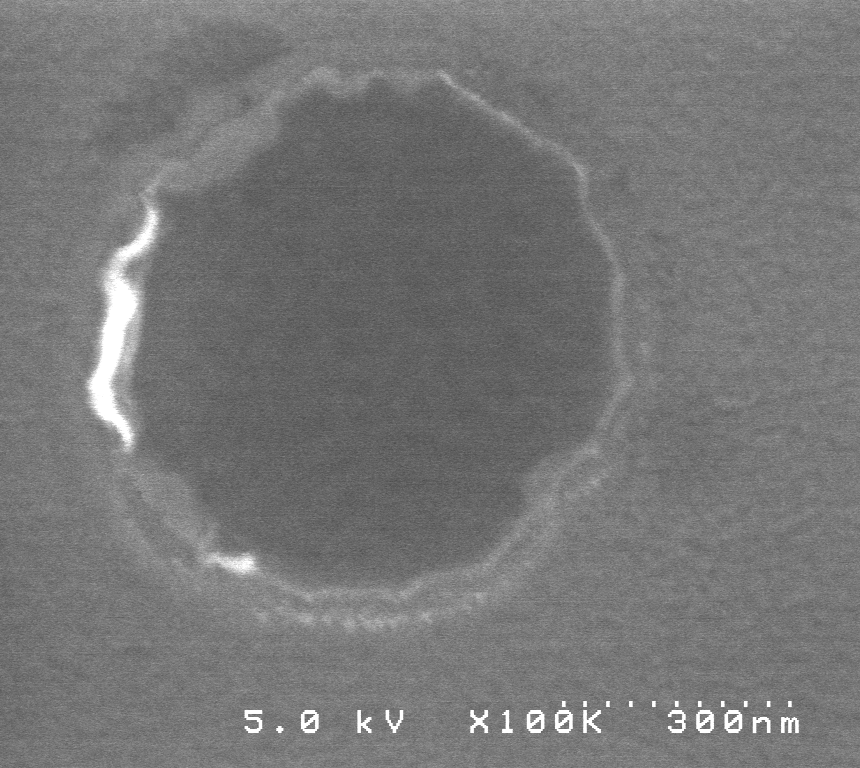
The thickness of isolation material is thinner on EB resist and thicker in area without EB resist. The etching a part of isolation might open the nano contact. In the same time, the remaining isolation material in areas without EB resist might be sufficient to isolate the top and back electrodes. Note: this method is sensitive to size of nano contact. It is efficient for nano contacts of diameter of 50 nm or less. It does not work for sizes larger than 100 nm.
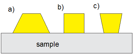
Fig.3 Cross-section of developed EB resist. Different shape of EB resist, which can be achieved by modulated -exposure method by optimizing the gap width and border exposure. |
a) not good; b) optimum for waveguides c) optimum for nano-magnets, waveguides and lift-off process |
In this case the EB resist is dissolved by hot NMP (T=70-120 deg C). The isolation material on top of the dissolved EB resist is mechanically broken and removed.
Nowadays many clean rooms have different types of lift-off machines, which are very efficient and simple to use. The yield of 100 % for nano contacts of different sizes can be reliably achieved.
Now a lift-off machine is a key-important machine for many nano technologies.
In some universities, the lift-off, which combines hot NMP + ultrasonic cleaner+ manual mechanical force on the sample surface, may be successful. However, the yield is poor for this lift-off method. In the case of nano contact, in which the materials with a weak adhesion is used (like metal+semiconductor), the ultrasonic cleaning destroys the nano contacts and it should be avoided at all steps of the fabrication technology.
For example, in order to a fabricate nanomagnet with diameter of 30 nm, it is better not to draw a nano dot of 30-nm diameter. Instead it is better to draw a larger nano dot with diameter of 100 nm with optimized border profile. Next, the diameter should be reduced by the slimming.
 Note: If you need a nano contact or a nano magnet of size of 30-50 nm or smaller, do not try to make EB pattern of this size. It is much better to make a pattern of larger size with optimized and controlled border shape. Next, to reduce the size to the required size by the slimming method. The result be incomparably better.
It is better to use a RIE machine for the slimming. In our clean room we have only a ICP-RIE machine. It can be used
Process 2=96+97
----------------------------
Rec. 96 (start)
P=8 Pa
O2=10.00 sccm
source/bias= 50W/80W
time = 20"
----------------------------
Rec. 97(main)
P=8 Pa
O2=10.00 sccm
source/bias= 50W/15W
time = 40" (it is optimized for each process)
The Ar milling is a critical step of this technology.
A smooth etching surface, a stable etching rate and minimal re-deposition are key parameters of the etching machine.
Since a etching rate of the Ar milling significantly depends on the sample temperature and may very during the etching, the stability and repeatability are important parameters of this machine.
For example, in order to fabricate a nano contact for spin-photon memory the precision of etching should be better than 0.1 nm. Otherwise, a very high resistance of the nano contact is result.
Au 2.9167 A/s=17.5 nm/min Fe 0.9375 A/s=5.6250 nm/min SiO2 1.05 A/s=6.3 nm/min (by Yamamoto SiO2 1.035 A/s=6.21 nm*min, 05.2009 - 5.71 nm/min)
Cr 0.9333A/s=5.6 nm/min MgO 0.5 A/s (old 0.210 A/s=1.26 nm/min (16/01 0.36 A/s) ) Co 0.922 A/s
GaAs 2.8 A/s=16.8 nm/min NiFe 1.01 A/s=6.06 nm/min CoFe 0.86 A/s=5.16 nm/min
Ti=0.439 A/s=2.6340 nm/min Co=0.922 A/s=5.53 nm/min Ga2O3 = 1.2 A/sec=7.2 nm/min
Al =8 nm/min AlO3 =1.5 nm/min (my) 1 nm/min (group), Si = 6.666 nm/min Ru=0.95-1 A/s (16/01 1.05 A/s) , Ta ~ 2.5 nm/min , FeBTb (15 W)=1 nm/ 15 ”=0.667 A/s Pt->1 nm=11”; Ir
 I am very thankful to Dr. Fukushima (AIST)
 ![]() for designing, making and allowing me to use the Ar-milling machine and the lift-off machine.
for designing, making and allowing me to use the Ar-milling machine and the lift-off machine.
I use Cr (5 nm):Au(70 nm)/Cr(5 nm) alignment marks. (Note: top Cr is used to increase adhesion of materials to marks. It is important to keep the marks in good shape for a long fabrication process)
In some cases a material from a sample is used for the marks. Sometimes only 5-8 nm of a metal is sufficient for alignment for both the EB lithography and the stepper.
Lift-off or Ar milling?
The Ar-milling is much better. The alignment precession increases about 2-8 times comparing to the case of marks fabricated by lift-off.
The lift-off-made marks should be used only in the case when a sample has a very weak and critical top protection.
The adhesion of a nano contact to the sample body is weak, because of its small sizes.
It can be easily be broken (disconnected from main body) by many reasons. Be careful.
Main reasons:
1) a large thermal gradient. Heat up and cool down your sample very slowly!!!
2) an ultrasonic cleaner. Avoid or minimize the use of an ultrasonic cleaner. Remember the operation frequency of the ultrasonic cleaner is important parameter and it should be optimized according to critical sizes of your nanomagnets.

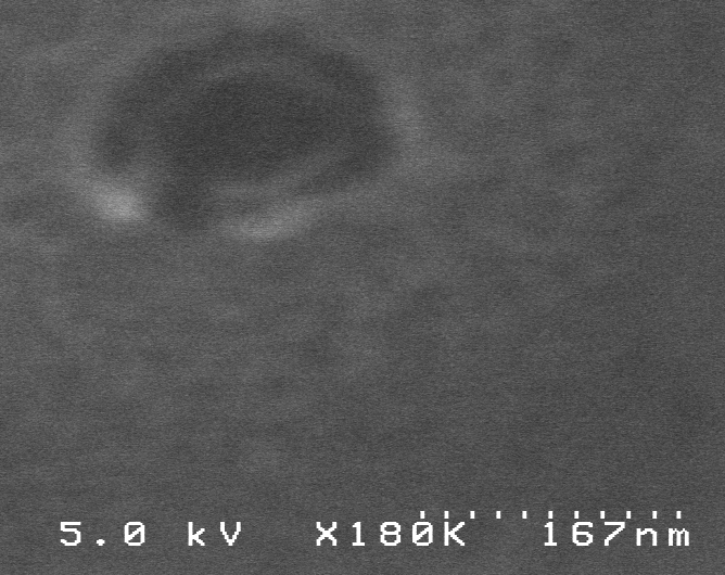
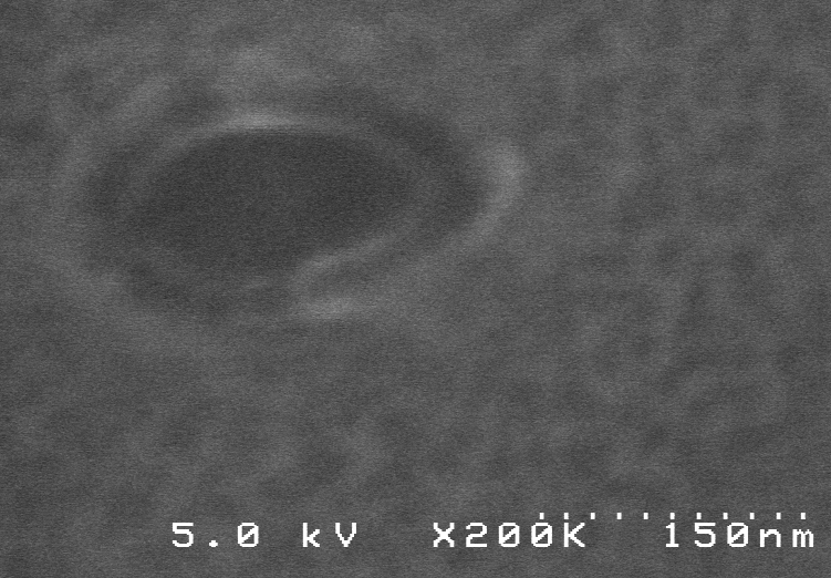
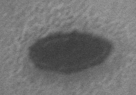
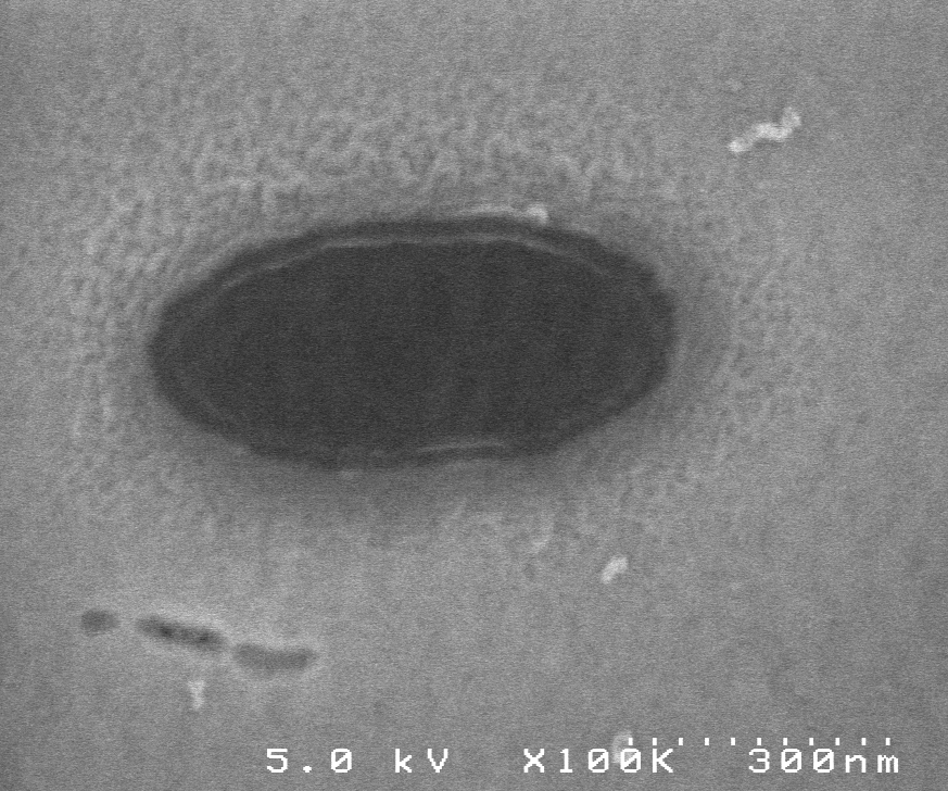
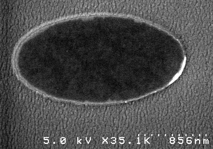
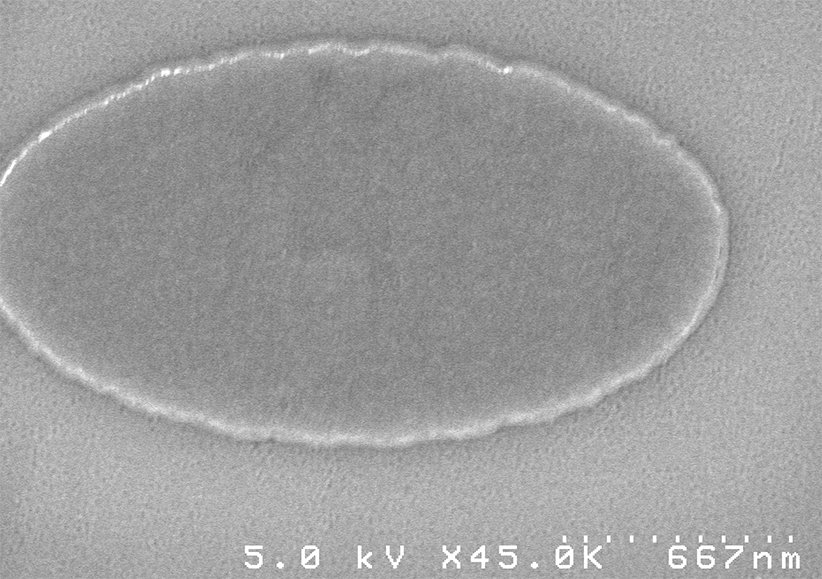
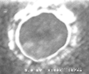
The darker area at center is top surface of nanomagnet
The brighter surrounding is SiO2 isolation layer
 |
 |
 |
 |
| 60 nm x 120 nm | 70 nm x 140 nm | 90 nm x 200 nm | 700 nm x700 nm |
 |
 |
 |
| 240 nm x570 nm | 1100 nm x1900 nm | 1100 nm x1900 nm |
j01 files for JEOL EB writer
EOS mode 8;
top number/10 is size, which needs to input during registration of j01 files
alignment marks (Cr(5 nm)/Au(70 nm)/Cr(5 nm)) should be made using reticle 10
Si nanowaguides
jdf files for JEOL EB writer
Matlab files to generate, to monitor, to modify .jdf and j01 files
Content
15 sec per one rotation
SiO2 100 W 100nm/55min=1.81 nm/min (0.1Pa Ar=9.5 O2=0.5)
SiO2 200 W 100nm/28min=3.57 nm/min (0.1Pa Ar=9.5 O2=0.5)
Co 100 W 85nm/60min=1.42 nm/min (0.5Pa Ar=30)
Cr 100 W 312nm/60min=5.2 nm/min (0.1Pa Ar=15)
Fe 100 W 60nm/90min=0.6667 nm/min (0.8Pa Ar=50)
Au 100 W 192nm/13min=14.77 nm/min (0.1Pa Ar=15)
Au 50 W 7.6 nm/min (0.1Pa Ar=15) zeng's 7.6 (metal) 7.9(SiO2) nm/min half 7.385
Cr 50 W 2.6 nm/min = 0.4333 A/s (0.1Pa Ar=15)
SiO2 HP 200 W 92.5nm/30min=3.08 nm/min (0.4Pa Ar=38 O2=2)
Ti 100 W 3 nm/min (0.1 Pa, Ar=15 sccm Fukushima)
Al 50 W 3 nm/min 100 W 6 nm/min 200 W 11.2 nm/min
Al2O3 100 W 1.04 nm/min (25 nm/24 min) 50 W=0.5 nm/min
Si 100 W 3.25 nm/min
TiO2 200 W 3 nm/min maybe 100 W 1.5 nm/min
Ru 100 W 32 nm/10 min 3.2 nm/ min
I will try to answer your questions as soon as possible
 The fabrication of the nano contact with diameter about 30 nm using EB lithography is challenging, but possible task. For successful and reliable fabrication all steps should be well optimized.