Dr. Vadym Zayets
v.zayets(at)gmail.com
My Research and Inventions
click here to see all content |

Dr. Vadym Zayetsv.zayets(at)gmail.com |
|
|
more Chapters on this topic:IntroductionTransport Eqs.Spin Proximity/ Spin InjectionSpin DetectionBoltzmann Eqs.Band currentScattering currentMean-free pathCurrent near InterfaceOrdinary Hall effectAnomalous Hall effect, AMR effectSpin-Orbit interactionSpin Hall effectNon-local Spin DetectionLandau -Lifshitz equationExchange interactionsp-d exchange interactionCoercive fieldPerpendicular magnetic anisotropy (PMA)Voltage- controlled magnetism (VCMA effect)All-metal transistorSpin-orbit torque (SO torque)What is a hole?spin polarizationCharge accumulationMgO-based MTJMagneto-opticsSpin vs Orbital momentWhat is the Spin?model comparisonQuestions & AnswersEB nanotechnologyReticle 11
|
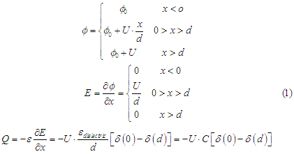
Charge Accumulation in a Conductor
Spin and Charge TransportThe charge accumulation may significantly change the properties of a conductor. In the case of a semicunductor, due to the charge accumulation the conductor even may change to be an isolator. There are :1) at the edge of dielectric, which is proportional to the applied voltage. It does not change the number of the localized electrons. (Capacitance of the MTJ)2) in the metal in the vicinity of the dielectric, which is proportional to the current flowing through the MTJ. There may be two contributions to this type of the charge accumulationa) charge accumulation due to the step of the conductivity.b) charge accumulation due to the tunnel resistance of the MTJ.3) charge accumulation due to a difference between work functions of metals of MTJ electrodes. It does not depends either on the allied voltage or the current.
When the charge is accumulated inside materials, the magnetic and electrical properties of material may be changed. The best example is a semiconductor. In the case when the charge is accumulated inside the semiconductor, its conductivity significantly changes and the semiconductor may change from conductor into dielectric and vice versa. A tunnel junction consists of two metal electrodes and dielectric between them. Because of a capacitance of the tunnel junction, a charge is accumulated in tunnel junction when the voltage is applied between electrodes. As it is shown in Fig. 1, this charge is accumulated on boundary of the dielectric. The polarization of the dielectric may induce the spin-orbit interaction, which may cause the voltage -induced the magnetization reversal (See here) When current flows through the tunnel junction, it induces a charge accumulation due to a change of the conductivity. , which is inside the metal. Therefore, it may influence the transport properties. The charge accumulation is within thickness in the metal, which equals about the mean-free path in the metal.
1. Capacitor.Classical model. Assumption of a point-like electrns in a metal.
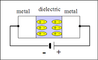
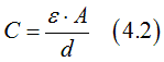
A capacitor consists of a dielectric inserted between two metals (Fig.1). In case when voltage is applied between metals, the charge is accumulated on the surface of dielectric.The charge accumulation is of opposite signs at two interfaces. The charge accumulated at electrodes of a capacitor is proportional to the applied voltage and it can be calculated as
where V is the applied voltage and C is the capacitance, q is the charge of an electron, N_accum is the number of the accumulated electrons The capacitance of a parallel-plate capacitor can be calculated as
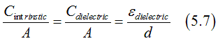
where A is area of the plates and d is the distance between plates and epsilon is permittivity of the dielectric.
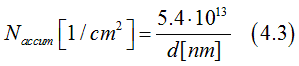
Result from Fig. 3: 1) The charge accumulation sharply increases when the thickness of dielectric becomes thinner. 2) To compare: The charge accamulated at surface state at GaAs/metal contact is about 1E12-1E14 1/cm2. The charge accamulated at surface state at H-terminated Si/metal contact is about 1E8-1E10 1/cm2. The charge accumulated at sides of a capacitor (See Fig. 3) is comparable to the charge accumulated at a semiconductor-metal contact.
The classical model In the classical model the electrons are assumed to be point-like particles. The charge accumulation in metal at contact with dielectric is assumed to be described by the delta function. The distribution of electrical potential, electrical field and charge density along the capacitor are
where epsilon and d is permittivity and thickness of the dielectric, , C is the capacitance and delta is the delta-function. The presented model. In the presented model the finite size of an electron in a metal is not ignored. The size of an electron approximatly equals to the mean-free path. Figure 4 shows the density of accumulated electron in the metal in the vicinity of the MgO tunnel barrier. To compare: For example, the largest possible doping concentation in GaAs is 4-6 E19 1/cm3 and in Si 1-2 E20 1/cm3. It is comparible with a charge accumulation in a metal near contact of the capacitor (Fig.4)
The ruduction of the capacitance due to a finite size of electrons in the metalScreening, the capacitance reduction
The capacitance of the charge accumulated region in the metal is
At frequancy f the resistance of the charge accumulated region in the metal
Tab
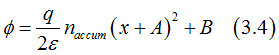
The electrical potential induced by a charge accumulation can be calculated the Gauss law. The Gauss law reads
where fi is the electrical potential, q is the electron charge. In the case when the potential varies only the x-axis and the charge accumulation constant, in the case of the constant charge accumulation Eq. (3.3) is solved as
Therefore the electrical potential in the charge accumulation region can be expressed as
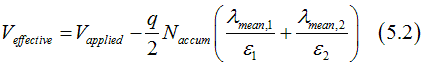
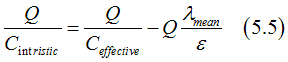
Since there is a potential drop in each metal, the effective voltage, which is applied to the dielectric, is reduced and it is calculated as
Since equal amounts of charge are accumulated at each side of the capacitor, the Eq. (5.1) is simplified to
or
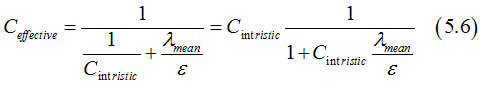
where Q is the charge accumulated at the capacitor The effective and intrinstic capacitances can be defined as
where the intristic capacitance of the capacitor, is the capacitance when the size of charge accumulation region in the metal can be ignored. Using definitions Eq. (5.4), Eq. (5.3) can be written as
the effective capacitance can be calculated as
in the case of paralel-plate capacitor, the inntristic capacitance can be calculated as
The capacitance due the finite size of the charge accumulation region in the metal can be calculated as
The effective capacitance can be calculated asthe capacitance of two capacitors in series
2. Charge accumulation due to the different work functions of the metals
At contact of two metals the charge can be accumulated due to a difference of the work functions of the metals at sides of the contact.
The work functions is energy difference between vacuum level and the Fermi energy in the bulk of the metal. When two metals with different work functions are contacted, the electrons form the metals with smaller work functions (shallower Fermi level) flows into the metals with larger work function (deeper Fermi level). The accumulated charge makes the Fermi level the same in both metals. This type of the charge accumulation does not depend on a voltage applied to the contact or a current flowing through the contact.
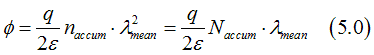
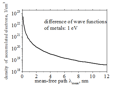
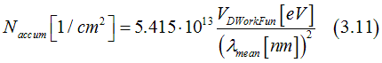
The difference between work functions of metal 1 and 2 equals can be calculated as The the density charge accumulation in the metals 1 and 2 in the vicinity of their contact
where V_DWorkFun is difference of the work functions of metal 1 and 2, epsilon is permittivity and lambda_mean is the mean-free path. The amount of the charge, which is accumulated at each side of the contact, is the same, but the charge accumulation is of the opposite signs. It is calculated as
Conclusions from Figure 11: 1) The charge accumulation sharply increases when the mean-free path decreases. Particulary the decrease is substantial when the mean-free path is less than 2 nm 2) The amount of the charge accumulation is comparible with the charge accumulation, which forms in a Schottky barrier. To compare: For example, the largest possible doping concentation in GaAs is 4-6 E19 1/cm3 and in Si 1-2 E20 1/cm3. It is comparible with a charge accumulation in a metal (Fig. 11 left) To compare: The charge accamulated at surface state at GaAs/metal contact is about 1E12-1E14 1/cm2. The charge accamulated at surface state at H-terminated Si/metal contact is about 1E8-1E10 1/cm2. The charge accumulated at a metal-metal contact (See Fig. 11 right) is comparable to the charge accumulated at a semiconductor-metal contact. Calculation of the charge accumulation due to the difference of the work functions of the metals. Eq. (3.7). Click to expand
In the case when the charge accumulation is constant within the charge accumulation region, the charge accumulation can be expressed as
where lambda_mean is the mean-free path in the metal 1 and 2. n_accum,1 is number of accumulated electrons in metal 1 and 2 The negative charge accumulation is equals to the positive charge accumulation in the metal 1, because the charge accumulation is only due to the move of the electrons from metal 1 to the metal 2. This condition is expressed as
The density of charge accumulation can be calculated from the Gauss law. The Gauss law reads
where fi is the electrical potential, q is the electron charge. In the case when the potential varies only the x-axis, Eq. (3.3) can be solved as
where A and B are constants. From Eqs. (3.4) and (3.2), the electrical potential fi in the vicinity of the contact can be expressed as
The potential difference due to the charge accumulation should be equal to the difference between the work functions of metals 1 and 2. From Eq.(3.5) the difference between work functions of metal 1 and 2 equals.
In the case when the permittivity is the same for both metals using Eq.(3.2) we obtain
In the case when the mean free path is the same for both metals Eq. (3.7) is simplified to
From the density of the accumulated electrons can be found as
where it is assumed epsilon=9.8 The total number of the electron accumulated at the contact interface can be found from integrating Eq. (3.9)
or
where it is assumed epsilon=9.8
Conclusions from Fig.12 1) The amount of the accumulated charge increases at both sides of the contact even if only in one metal the mean-free path decreases.
The limitation of the classical modelIn the descriptions of the charge accumulation in a metal within theclassical model hits its limits for charge accumulation at a contact.
|
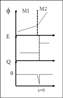 |
Fig.2 Electrical potential, electric field and charge distribution along contact between two metals |
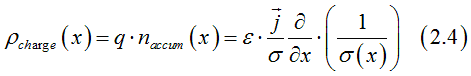
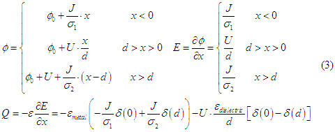
Let us consider a contact between two metals, which have equal work function, but different conductivity. The distribution of electrical potential, electrical field and charge density along the contact are
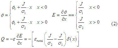
It should be notice the charge accumulation occurs only when there is a current through the contact.
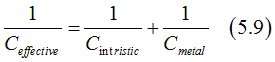
3. Charge accumulation due to the contact resistance
As it is shown in Fig.4, in the case of tunnel junction, there are two different charge accumulations. One is in the metal and another one is in the dielectric. The charge accumulation in the dielectric occurs due to the capacitance of the junction. This accumulation does not affect the transport properties of the metals. The charge accumulation in the metal occurs due to the tunneling current. This accumulation might significantly affect transport properties of the metals. The similar charge accumulation in the metal can occur due to a difference of work functions of metals. It also does affect the transport properties of the metals. In the case when metals have equal work function, but different conductivity and the tunneling current through contact is J, the distribution of electrical potential, electrical field and charge density along the tunnel junction are
 |
Fig.4 Charge accumulated in a tunnel junction. Charge accumulated in dielectric (yellow) due to junction capacitance. Charge accumulated in metals (green) due to (1) the screening of charge in the dielectric; (2) due the difference of the work functions of metal electrodes and (3) the current flow |
where 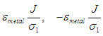 are the accumulated charge in metal 1 and metal 2, respectively.
It should be noticed that the charge accumulation in the metals is induced by the tunneling current J.
I will try to answer your questions as soon as possible