Dr. Vadym Zayets
v.zayets(at)gmail.com
My Research and Inventions
click here to see all content |

Dr. Vadym Zayetsv.zayets(at)gmail.com |
|
|
more Chapters on this topic:IntroductionTransport Eqs.Spin Proximity/ Spin InjectionSpin DetectionBoltzmann Eqs.Band currentScattering currentMean-free pathCurrent near InterfaceOrdinary Hall effectAnomalous Hall effect, AMR effectSpin-Orbit interactionSpin Hall effectNon-local Spin DetectionLandau -Lifshitz equationExchange interactionsp-d exchange interactionCoercive fieldPerpendicular magnetic anisotropy (PMA)Voltage- controlled magnetism (VCMA effect)All-metal transistorSpin-orbit torque (SO torque)What is a hole?spin polarizationCharge accumulationMgO-based MTJMagneto-opticsSpin vs Orbital momentWhat is the Spin?model comparisonQuestions & AnswersEB nanotechnologyReticle 11
more Chapters on this topic:IntroductionTransport Eqs.Spin Proximity/ Spin InjectionSpin DetectionBoltzmann Eqs.Band currentScattering currentMean-free pathCurrent near InterfaceOrdinary Hall effectAnomalous Hall effect, AMR effectSpin-Orbit interactionSpin Hall effectNon-local Spin DetectionLandau -Lifshitz equationExchange interactionsp-d exchange interactionCoercive fieldPerpendicular magnetic anisotropy (PMA)Voltage- controlled magnetism (VCMA effect)All-metal transistorSpin-orbit torque (SO torque)What is a hole?spin polarizationCharge accumulationMgO-based MTJMagneto-opticsSpin vs Orbital momentWhat is the Spin?model comparisonQuestions & AnswersEB nanotechnologyReticle 11
more Chapters on this topic:IntroductionTransport Eqs.Spin Proximity/ Spin InjectionSpin DetectionBoltzmann Eqs.Band currentScattering currentMean-free pathCurrent near InterfaceOrdinary Hall effectAnomalous Hall effect, AMR effectSpin-Orbit interactionSpin Hall effectNon-local Spin DetectionLandau -Lifshitz equationExchange interactionsp-d exchange interactionCoercive fieldPerpendicular magnetic anisotropy (PMA)Voltage- controlled magnetism (VCMA effect)All-metal transistorSpin-orbit torque (SO torque)What is a hole?spin polarizationCharge accumulationMgO-based MTJMagneto-opticsSpin vs Orbital momentWhat is the Spin?model comparisonQuestions & AnswersEB nanotechnologyReticle 11
|
Parameters of magnetic materials. MgO-based MTJ
Spin and Charge TransportA MgO-based magnetic tunnel junction (MTJ) is important for many Spintronics application. This page describes the reference date for MTJ with a MgO tunnel barrier.
|
|
||||||
| MTJ consists of two ferromagnetic metals separated by a thin isolator. The ferromagnetic metals are not exchange- coupled, therefore their magnetization can be changed independently. The isolator is very thin (~1 nm), therefore a tunneling current can flow between metals | ||||||
| MTJ is used as a memory cell in Magnetic Random Access Memory | ||||||
| click on image to enlarge it |
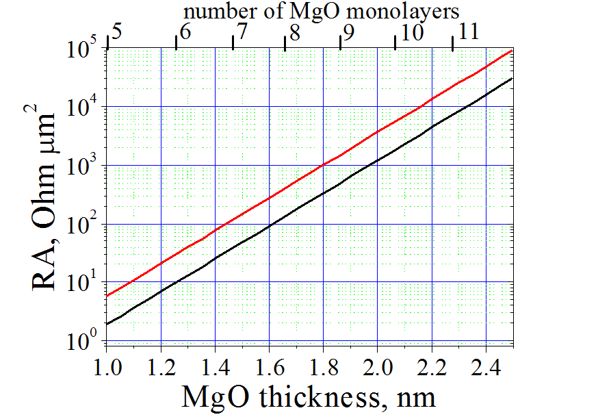
The tunneling resistance exponentially proportional to the the MgO barrier thickness. The resistance-area product for Fe/MgO/Fe can be expressed as (See here)
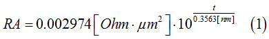
Note: near each two monolayers the resistivity increases 10 times
Note: For MgO thickness near 1.0 nm , the MTJ resistance a little larger than it is expressed by fitting (Eq.(1)).
Break-down voltage of MgO-based MTJ
For MTJ grown by MBE or by sputtering+anneal, the break-down voltage is 0.7-1 V/nm=700-1000 MV/m.
The break-down voltage of a thin-film MgO is near 1000 times larger than the break-down voltage of a bulk MgO, which is typical 6-10 MV/m and for best sample it is 151 MV/m
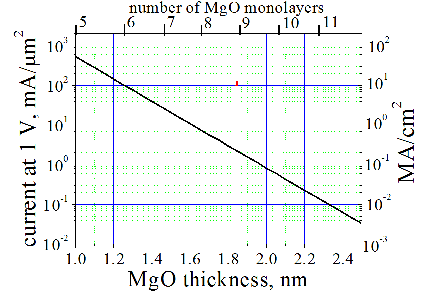
Maximum current through MgO-based MTJ
Figure 2 shows the current, which flows through the MTJ under 1 V. The red line shows the typical critical current, above which the current-induced magnetization reversal occurs.
For the current-induced magnetization reversal, it is desirable to have a MTJ with MgO barrier as thinner as possible.
Fig.1. Resistance-area product (RA) of Fe/MgO/Fe magnetic tunnel junction (MTJ) The blue line shows RA for the case when the magnetizations of the electrodes are parallel. The red line shows RA for the case when the magnetizations are antiparallel. click here or on image to enlarge it |
Fig.2 Current through Fe/MgO/Fe MTJ at applied voltage of 1 V The red line shows the typical critical current above which current-induced magnetization reversal occurs. click here or on image to enlarge it |
|
 |
In metals the electron transport is the running-wave electron current.
Through the tunnel barrier, the electron transport is the scattering current.
Only one scattering event is sufficient for an electron to pass from electrode to another electrode through the tunnel barrier. Such scattering electron current is called the ballistic electron current.
![]() Q. If a MTJ with a thinner MgO layer is better, why not to make MTJ with MgO thickness of 4 or 3 or even 2 monolayers? Is the film roughness the problem?
Q. If a MTJ with a thinner MgO layer is better, why not to make MTJ with MgO thickness of 4 or 3 or even 2 monolayers? Is the film roughness the problem?
![]() A. The fabrication technology of MTJ (MBE and sputtering) becomes very matured. A MgO barrier with roughness less 1 monolayer can be fabricated.
A. The fabrication technology of MTJ (MBE and sputtering) becomes very matured. A MgO barrier with roughness less 1 monolayer can be fabricated.
![]() Minimal thickness of of MgO is ~1 nm (5 monolayers)
Minimal thickness of of MgO is ~1 nm (5 monolayers)
In case of a MTJ with thickness thinner than 5 monolayer, magneto-resistance (MR) ratio sharply decreases. It is not because of limitations of the fabrication technology, but it is because of the features of the electron transport
![]() The high MR in MgO-based MTJ is due to spin-dependent features of the ballistic current (scattering current). When the MgO thickness becomes thinner than 5 monolayers, the refractivity of the tunnel barrier becomes nonzero (See here) and the running-wave electrons can pass from one electrode to another electrode. Since the running-wave electron current is significantly more efficient than the scattering current, the running-wave electron current shunts the scattering current and the MR sharply decreases.
The high MR in MgO-based MTJ is due to spin-dependent features of the ballistic current (scattering current). When the MgO thickness becomes thinner than 5 monolayers, the refractivity of the tunnel barrier becomes nonzero (See here) and the running-wave electrons can pass from one electrode to another electrode. Since the running-wave electron current is significantly more efficient than the scattering current, the running-wave electron current shunts the scattering current and the MR sharply decreases.
Fig.3. Capacitance of Fe/MgO/Fe MTJ click here or on image to enlarge it |
Fig.4 Comparison of the Capacitor resistance with the Ohmic resistance of The black line shows the Ohmic resistance-area product of the MTJ. Other lines show the capacitor click here or on image to enlarge it |
|
 |
The MTJ is a parallel - plate capacitor and its capacitance properties should not be ignored.
The capacity can be calculated as
where epsilon is permittivity of MgO, A is the area of MTJ, d is the MgO thickness.
The capacitor resistance at the frequency f can be calculated
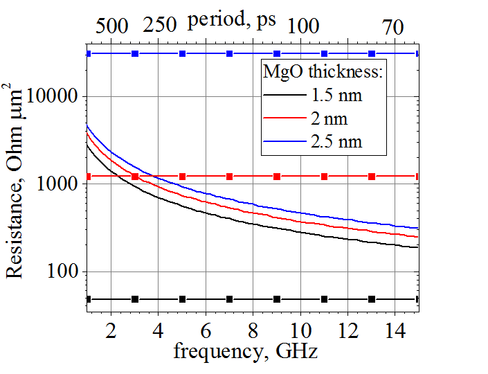
Fig.5. Capacitance resistance The top x-axis shows the period of the corresponded frequency (bottom x-axis) click here or on image to enlarge it |
Fig.6 Capacitance resistance
click here or on image to enlarge it |
|
 |
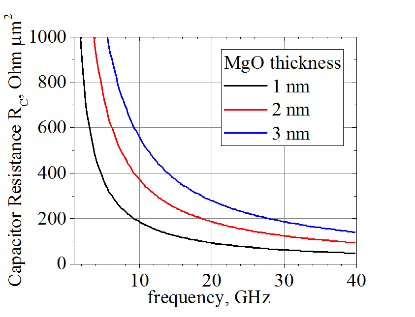
At high frequency (f >1 GHz), the capacitance resistance  can shunt the tunnel resistance and the tunnel magneto-resistance (TMR) is reduced. For example, when the capacitance resistance is equal to the tunnel resistance, the TMR is reduced in 2 times compared to the TMR at DC.
 For a high TMR the tunneling resistance should be larger than the capacitor resistance of the MgO !!!!
Figure 5 compares the capacitance resistance with the tunneling resistance for different thicknesses of the Fe/MgO/Fe MTJ.
For MgO thicker than 2 nm the high TMR is only possible at lower a frequency. For MgO thickness of 2 nm, the maximum frequency of a high TMR is about ~1 GHz.
For MgO thinner than 1.6 nm the TMR is high even for frequencies above 10 GHz.
From Fig.6, the MTJ with resistance smaller than 50 Ohm*um2 may have a high MR even for frequencies above 40 GHz.
Note: the resistance of MTJ, which is used for MRAM, is 1-10 Ohm*um2 (MgO thickness ~ 1 nm). For MgO thinner than 1 nm, the current of the running-wave electron becomes comparable with the scattering current and TMR sharply drops.
| g-factor of conduction band electrons: | ||||||||||||||||||||
|---|---|---|---|---|---|---|---|---|---|---|---|---|---|---|---|---|---|---|---|---|
|
| g-factor of valence band electrons: | ||||||||||||||||||||
|---|---|---|---|---|---|---|---|---|---|---|---|---|---|---|---|---|---|---|---|---|
|
Paramagnetic (Si unit)
| FeO | Pt | Al | W | Cr | Ti | ||
| 720×10−5 | 26×10−5 | 2.2×10⁻⁵ | 6.8×10⁻⁵ | 31.3×10⁻⁵ | 18.1×10⁻⁵ |
Diamagnetic (Si unit)
| Ag | Cu | Au | Si | Al2O3 | |||
| -2.6×10⁻⁵ | -1×10⁻⁵ | -3.44×10⁻⁵ | -0.41×10⁻⁵ | -1.81×10⁻⁵ |
unit conversion: (CGS-emu=Si-unit/4pi)
| g-factor of conduction band (bulk) electrons: | ||||||
|---|---|---|---|---|---|---|
|
| 4piM (kGauss) | ||||||||
|---|---|---|---|---|---|---|---|---|
|
FMR: magnetic field (Gauss) for 9.8 GHz |
||||||||
|---|---|---|---|---|---|---|---|---|
|
relaxation parameters
Fe 57 MHz ( alfa= 0.002)
Ni 220 MHZ
Co 170 MHz
Py 114 MHz
;;;;;;;;;;;;;;;;;;;;;;;;;
for YIG width of FMR resonance
0.15 Oe -0.2 Oe
Strains
The perpendicular-to-plain magnetization may also increase (decrease) due to strain.
When a thin film is grown on a substrate of different lattice constant, the film is strained.
When the lattice parameter of the film is larger than that of the substrate, the strains are tensile. The effective magnetic field of the spin-orbit interaction, which induced by the strains, is directed perpendicularly to the film plane.
When the lattice parameter of the film is larger than that of the substrate, the strains are compressive. The effective magnetic field of the spin-orbit interaction, which induced by the strains, is directed in plane.
Strain relaxation and the critical thickness.
The strain field, which acts on the film-substrate interface, is linearly proportional to the film thickness. The thin film has the in-plane lattice parameter the same as that of the substrate. As the film thickness increases the strain field, which acts on the interface, increases. At some thickness the strain field becomes sufficient to create a dislocation at interface. This thickness is called the critical thickness. The dislocations reduce the strain in the film. The process of the creation of the dislocation is called the stain relaxation mechanism.
The critical thickness depends on the crystal quality of the film and the strain relaxation mechanism. Approximately, the critical thickness hcritical can be calculated from relation:
![]()
notice: Eq. (3) is valid only for high-crystal quality low-defect-density materials. Otherwise, the ratio (3) becomes smaller than 0.7.
Example 1. AlGaAs (001)on GaAs(001)
The lattice constant of AlGaAs (x=0.5) is 0.069 % larger than the lattice constant of GaAs.
The strains are compressive. The critical thickness approximately equals to 1 um.
Example 2. InGaAs(001) on GaAs(001)
The lattice constant of InGaAs (x=0.5) is 3.582 % larger than the lattice constant of GaAs.
The strains are compressive. The critical thickness approximately equals to 19.5 nm.
Example 3. Fe(001) on MgO(001)
The lattice spacing of MgO (001) in [110] direction is 3.74 % smaller than lattice spacing of Fe (001) in [100] direction.
For Fe film on MgO, the strains are tensile. For MgO film on Fe, the strains are compressive.
The critical thickness in both cases approximately equals to 18.7 nm.
3.74% of tensile strains in Fe correspond to mechanical tensile stress of 7.44 GPa
3.74% of strains in MgO correspond to mechanical compressive stress of 9.3 GPa. It is significantly larger than the elastic limit of MgO of 160 MPa, and compressive Strength of 1.6 GPa
| Fe | Ta | Cr | V | Cu | W | Co(bcc) | Mo | Nd | ||
|---|---|---|---|---|---|---|---|---|---|---|
| lattice constant, Å | 2.870 | 3.310 | 2.880 | 3.020 | 2.88 | 3.160 | 2.83 | 3.150 | 3.300 | |
| along [110], Å | 2.03 | 2.34 | 2.036 | 2.135 | 2.036 | 2.234 | 2.00 | |||
| mismatch with MgO | -3.63% | 11.1% | -3.3% | 1.4% | -3.3% | 6.1% | -4.98% | |||
| critical thickness on MgO | 4 nm | 1.3 nm | 4.5 nm | 11 nm | 4.5 nm | 2.5 nm | 3 nm | |||
| mismatch with Fe, % | 0 | 15.29% | 0.32% | 5.2% | 0.32% | 10 % | -1.423% | |||
| critical thickness on Fe, nm | 0 | 1 nm | 50 nm | 2.9 nm | 50 nm | 1.5 nm | 10.5 nm |
note: for high crystal quality (semiconductors) Critical Thickness*Strain=0.7
For calculation in table, it was used Critical Thickness*Strain=0.15
Note: 2D growth is assumed for the calculations of the critical thickness. 3D growth is the case when the lattice mismatch is large.
Note: Co(bcc) is metastable, but FeCo (bcc) is stable even for high (75%) Co constant.
Note: Cu(bcc) is metastable
lattice constant of FeCo =2.87 A for x=0, it is near constant till 20 %, next it reduces to 2.83 A for BCC Co
Note: The critical thickness depends on the density of the dislocations in the substrate.
When the film thickness reaches the critical thickness the strains start to relax by generating the misfit and treading dislocations.
The misfit dislocations (less evil) are generated at the interface between metals. Usually they influence the transport in the metal film weakly.
The threading dislocations are generated through the bulk of the film. They breaks periodicity of the metal, which is responsible for the band structure of the metal. Therefore, the vicinity of a threading dislocation the properties of the metal might be significantly different.
Whether the threading or misfit dislocations are generated during the strain relaxation depends on the film growth conditions.
Try to avoid the threading dislocations in your film !!!
MgO lattice constant a = 4.212Å (a/2=2.106Å)
Si=5.431 Å (a/2=2.7155) (along [110] 1.92 Å )
Ge=5.66 Å (a/2=2.83) (along [110] 2.001 Å )
GaAs= 5.65325 Å (a/2=2.826625 ) (along [110] 1.9987 Å )
| Fe | Ta | Cr | V | W | Cu | |
|---|---|---|---|---|---|---|
| lattice constant, Å | 2.870 | 3.310 | 2.880 | 3.020 | 3.160 | 2.88 |
| along [110] | 2.03 | 2.34 | 2.036 | 2.135 |
| Ni | Pt | Au | Cu | Al | Pd | Ag | Rh | Pb | Co | |
|---|---|---|---|---|---|---|---|---|---|---|
| lattice constant, Å | 3.520 | 3.920 | 4.080 | 3.610 | 4.050 | 3.890 | 4.09 | 3.800 | 4.950 | 3.544 |
| a/2, Å | 1.96 | 2.040 | 2.025 |
| Co | Ru | Ti | Mg | Tb | Gd | Zn | Tc | Y | Zr | Sc | Ta | ||
|---|---|---|---|---|---|---|---|---|---|---|---|---|---|
| lattice constant, Å | 2.51-2.59 | 2.700 | 2.950 | 3.210 | 3.600 | 3.640 | 2.66 | 2.740 | 3.650 | 3.230 | 3.310 | 2.950 | |
| a/2, Å | |||||||||||||
| c/a ratio | 1.584 | 1.588 | 1.624 | 1.581 | 1.588 | 1.604 | 1.571 | 1.593 | 1.594 |
BCC cell consists of 2 net atoms, The bcc unit cell has a packing factor of 0.68.
FCC cell consists of 4 net atoms. The bcc unit cell has a packing factor of 0.74.
hcp cell consists of 6 net atoms. The bcc unit cell has a packing factor of 0.74.
Young's modulus (tensile strain) & Bulk module (compressive strain)
(note): The force needed to expand a material by a certain distance differs from the force needed to compress it by the same distance.
| SiO2 | Al | Au | Ti | Cu | Pt | Ta | Fe | Co | W | Ru | Ir | MgO | |
|---|---|---|---|---|---|---|---|---|---|---|---|---|---|
| Young's modulus (tensile strain), GPa | 68 | 69 | 79 | 110 | 118 | 168 | 186 | 210 | 209 | 400 | 447 | 528 | 270-330 |
| Bulk module (compressive strain), GPa | 35 | 76 | 220 | 110 | 140 | 230 | 200 | 170 | 180 | 310 | 220 | 320 | 250 |
MgO bulk elastic properties
Compressive Strength 800-1600 MPa
Elastic Limit 80-166 MPa
Hardness 5-7 GPa
Breakdown Potential= 6-10 MV/m=0.006-0.01 V/nm
Conductivities (S/m)
| Silver | 6.30E+07 |
| Copper | 5.96E+07 |
| Gold | 4.10E+07 |
| Aluminium | 3.50E+07 |
| Tungsten | 1.79E+07 |
| Co | 1.66E+07 |
| Nickel | 1.43E+07 |
| Ru | 1.40E+07 |
| Iron | 1.00E+07 |
| Platinum | 9.43E+06 |
| Tin | 9.17E+06 |
| Cr | 7.87E+06 |
| Ta | 7.40E+06 |
| Carbon steel (1010) | 6.99E+06 |
| Lead | 4.55E+06 |
| Titanium | 2.38E+06 |
| Stainless steel | 1.45E+06 |
| titanium Nitride | 1.42-3.33E6 |
To obtain a highest-crystal-quality MTJ, it is better to avoid any strain relaxation either in metal or MgO barrier.
The critical thickness for the strain relaxation for the MgO is thin. On a Fe substrate or a partially-relaxed Fe, the critical thickness is less than 0.8 nm.
Additionally, it seems that magneto-transport property are better in MTJ, in which the MgO barrier is unstained and with a minimum amount of the dislocations. For example, a highest TMR was obtained in a MTJ, in which MGO lattice parameter is close to the lattice parameter of bulk MgO. (See APL 93, 082508(2008))
For this purpose a multi-layers, which lattice-matched to MgO are useful.
The bulk lattice parameter of MgO
MgO lattice constant a = 4.212Å (a/2=2.106Å)
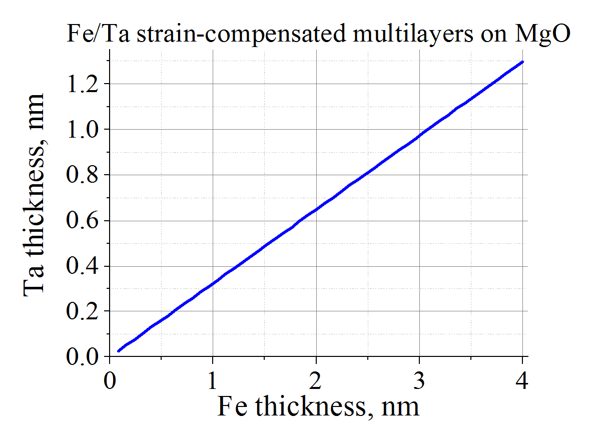
Fe/Ta strain-compensated multi layers on MgO substrate click here or on image to enlarge it |
Cr/Ta strain-compensated multi layers on MgO substrate click here or on image to enlarge it |
|
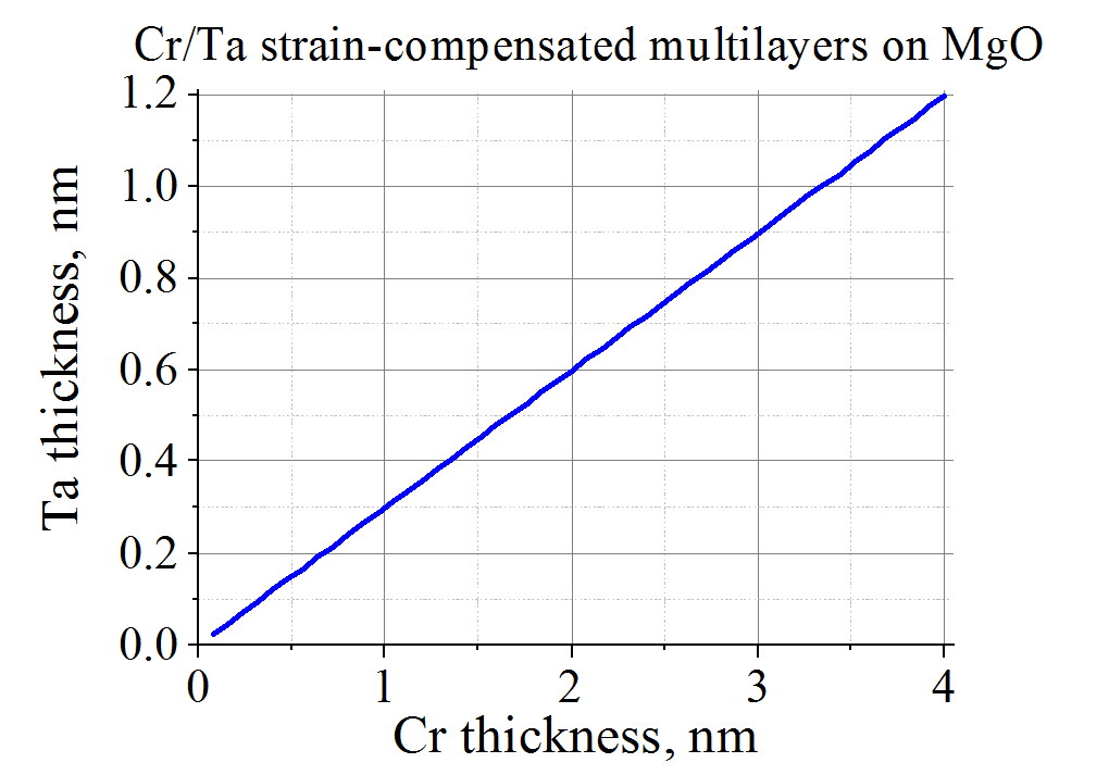 |
In order to match the lattice parameter of the MgO, at least one metal with a larger lattice parameter and at least one metal with a smaller lattice parameter have to be used.
Fe (BCC) = 2.870Å (along [110] 2.03 Å ). Lattice mismatch -3.6%. Strains are tensile.
Ta (BCC)= 3.310 Å (along [110] 2.34 Å ). Lattice mismatch 11.1 %. Strains are compressive.
Strain-compensated multilayer should satisfy
tFe*3.6=tTa*11.1
For example, (Fe(1.5 nm)/Ta(0.49 nm))10 multilayer can be used as a lattice matched buffer layer on a MgO substrate.
Cr (BCC) =2.880 A (along [110] 2.036 Å ). Lattice mismatch -3.32%. Strains are tensile.
Ta (BCC)= 3.310 Å (along [110] 2.34 Å ). Lattice mismatch 11.1 %. Strains are compressive.
Strain-compensated multilayer should satisfy
tCr*3.32=tTa*11.1
For example, (Cr(1 nm)/Ta(0.3 nm))20 multilayer can be used as a lattice matched buffer layer on a MgO substrate
The effect describes the change of shape of a ferromagnetic material when its magnetization changes.
The origin of the effect
Magnetostatic interaction between domains in the ferromagnetic materials. When shape, size, magnetization inside domains changes, the strength of the magnetostatic interaction between domains changes and the lattice contracts or expands.
Note: in a single-domain nanomagnet the magnetostriction of this type does not exists.
Materials
CoFeB 20:60:20 magnetostriction coefficient is 3.7E-5
Terfenol-D (TbxDy1-xFe2)
The magnetostriction of the Terfenol-D generates strains 100 times greater than traditional magnetostrictive, and 2-5 times greater than traditional piezoceramics.
For typical transducer and actuator applications, Terfenol-D is the most commonly used engineering magnetostrictive material.
Elastic properties (Tb0.3Dy0.7Fe1.92)
Young's Modulus=25-35 GPa
.
![]() Hi sir, Good afternoon. Myself Eswar.H doing phd in the field of non linear dynamics especially in Spin Torque Nano Oscillator
Hi sir, Good afternoon. Myself Eswar.H doing phd in the field of non linear dynamics especially in Spin Torque Nano Oscillator
I had one doubt sir? Typically Spin Torque Nano Oscillator consists of three layers (i.e.) 2 ferromagnetic layer separated by a non magnetic spacer. My doubt was
1)On what basis they fix the thickness of spacer,Pinned layer, and free layer (everything in nano-meter range)? Is there any physics behind that?
2)or Is there any ratio between the all three layers? (Example: 2:1 ratio between pinned and free layer) Likewise?
please tell me sir.
A. The resistance of a tunnel barrier sharply increases with a slight increase of the thickness of the tunnel barrier.
For Fe/MgO/Fe See Fig.1 here
https://staff.aist.go.jp/v.zayets/spin3_46_MgO.html
For MgO thinner than 1 nm, there is no tunneling and MR.
For 3 nm of MgO the resistance is too high and it is even hard to measure the resistance.
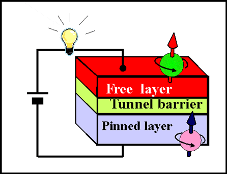
The STO (spin-torque oscillator) needs a high current, therefore the thinnest-possible MgO thickness( about 1 nm) is used.
Thickness of the free layer is fixed about 2 nm.
There is an effective spin-torque only within thickness about 1 nm in the vicinity of MgO. For a thinner free-layer, it easier to make its magnetization to precess with smaller spin-torque and a smaller current.
The pin layer also experiences the spin-torque, but its magnetization should not precess. Therefore, it should be a thicker as possible. However, the magnetization of a thick film breaks into domains. Also, the magnetic field from a thick magnetic layer undesirably affect the free layer. It is not good. Therefore, an antiferromagnetic layer is used for pinning.
Q.![]() Now i understood the concept clearly. Sir but you explained it for a Tunneling Magneto Resistance. Please explain me what happens if we replace the insulating barrier by a conducting spacer (i.e.) for Giant Magneto Resistance (Non-magnetic conducting spacer)
Now i understood the concept clearly. Sir but you explained it for a Tunneling Magneto Resistance. Please explain me what happens if we replace the insulating barrier by a conducting spacer (i.e.) for Giant Magneto Resistance (Non-magnetic conducting spacer)
1) In case of GMR how we fix the thickness of free and fixed layer and spacer? Please explain the physics behind that?
2)Is there any ratio behind the thickness of all three layers?
A.
For the GMR structure the story is almost the same as for the TMR structure.
The reasons for optimum thicknesses of pin and free layers are the same.
The physics the same:
The free layer:
Thickness should be smaller than a spin diffusion length in this layer (~ 1-2 nm). Therefore, whole layer should experience the spin transfer torque.
It should be very thin, but It could not be too thin.
The mobility of Fe atoms on the most of surfaces are high, a thin Fe film tends clustering and it is difficult to make a smooth continuous Fe layer thinner than 1 nm. For the case of amorphous FeB (or FeCoB) is better, but still it is difficult to make a thin continuous film.
The pin layer:
The thickness should be thicker than the spin diffusion length. Therefore, only a part of layer experiences the spin transfer torque and the magnetization of the pin layer should not be reversed by current.
It should be thick, but it could not be too thick.
The magnetic field of this layer should be minimized. It should not affect the free layer.
It should be a thin enough to be in a single-domain state.
The spacer layer:
The spacer layer separates the free and the pin layers. Therefore, there is no exchange interaction between them. The magnetization direction of each layer can be independent from another layer.
Generally speaking, the thickness of the spacer layer should be thicker than the length of interlayer exchange interaction, which is a few interatomic distances.
However, the thickness of the spacer layer should be substantially thicker.
It could not be thicker than the spin diffusion length in the spacer layer. Therefore, a metal with a long spin diffusion length (like Cu) is used as the spacer material.
The reasons why the spacer layer should be thick are:
1) GMR ratio should be high. Output of STO is proportional to GMR ratio.
2) Even though there is no direct exchange interaction between localized electron at distances longer than a few atomic monolayer, there is another longer-range exchange interaction, which mediated by conduction electrons. Such exchange coupling exists only in GMR structure, but not in TMR. The spacer of TMR structure is isolator, it does not have the conduction electrons. The range of such interaction is about the size of conduction electrons, which equals to the mean-free-path. For example, in Co:Ru:Co such interaction is strongest at 0.9 nm of Ru thickness
3) The spin torque is larger in the case of a thicker spacer layer if the thickness is thinner than spin diffusion length.
For higher spin torque, the conductivity type should be changed from bulk-type to the interface type.
In the bulk of a metal, there is almost no spin drift and no spin-torque.
In the case of TMR, the conductivity by the tunneling is different from the bulk conductivity.
For GMR with a thin spacer, the conductivity is still bulk like, therefore the spin torque is small.
----------------
There is no a "magic" ratio between thicknesses of the layers. However, for each choice of metals the thicknesses of each layers should be optimized, especially for the GMR structure.
I will try to answer your questions as soon as possible