Dr. Vadym Zayets
v.zayets(at)gmail.com
My Research and Inventions
click here to see all content |

Dr. Vadym Zayetsv.zayets(at)gmail.com |
|
|
Spin -Photon memory
Nano- and micro- fabrication technologyI have developed the advanced and unique fabrication technology for the spin-photon memory. Ultra-low resistance between a nanomagnet and semiconductor and the smallest- possible size of nanomagnets are required features of the fabrication technology.
|
|
||
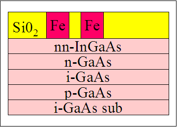
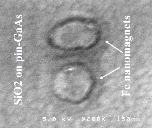
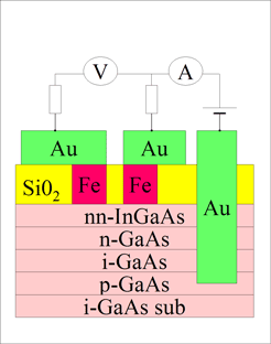
Fig.1 (left) Cross-sectional view of the spin-photon memory; (right) Top view. SEM image of two Fe nanomagnets on the top of pin-GaAs. SiO2 is used for the isolation. The typical diameter of a nanomagnet is 70 nm and a gap between nanomagnets is 30 nm. |
Figure 1 (left) shows the design of the spin photon memory with two Fe nanomagnets. One nanomagnet is used to store data. Another nanomagnet is used for data reading. In order to reduce the minimum intensity of optical pulse required for the recording, the sizes of the nanomagnets should be smallest possible. The distance between nanomagnets should be very short (at least it should be shorter than the spin diffusion length in GaAs).
For some samples, FeCo:MgO:FeCo magnetic tunnel junction (MTJ) is used instead of the Fe nanomagnets.
The lowest contact resistance between the Fe nanomagnet and the GaAs is crucially important for the operation of the memory. The lowest resistance is important to ensure a sufficiently short spin injection time. The requirement of the lowest contact resistance can be understood as follows. In a semiconductor pin-photodetector the photo voltage, which is induced by an optical pulse, can not exceed the value of semiconductor bandgap. Therefore, in GaAs pin photodiode the photovoltage can not exceed ~1 V. In the best case the threshold current for magnetization reversal in Fe is about 10 mA/um2(=1E6 A/cm2). Therefore, the maximum contact resistance, when still it is possible to reverse magnetization of nanomagnet by photocurrent, is 1V/10 mA/um2=100 Ohm um2.
In the fabrication technology, which I have developed, the typical contact resistance is 20 Ohm um2. (Even I can go to down to 10 Ohm um2). For comparison, the lowest resistance of all-metallic MTJ for MRAM application is a few Ohm um2.
|
||
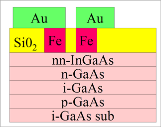
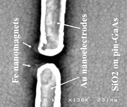
Fig.2 (left) Cross-sectional view of the spin-photon memory with Au nanoelectrodes; (right) Top view. SEM image of two Fe nanomagnets. Each nanomagnet connected by Au electrode. The nanomagnets are covered by nanoelectrodes. Still some parts of the nanomagnets can be seen. |
|
||
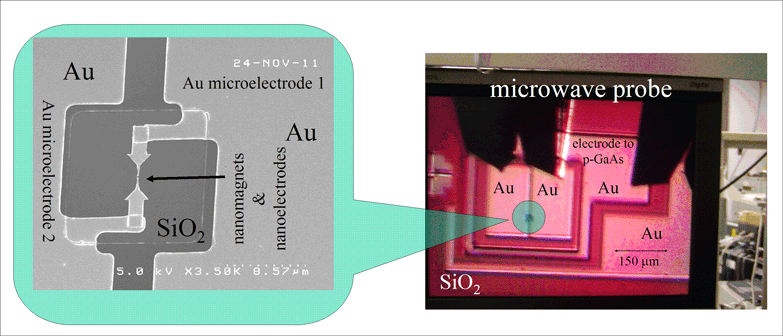
Fig.3 (left)Cross-sectional view of measurement setup for spin photon memory. The right Au contact is contact to p-GaAs. Its fabrication was optimized so it is not in contact with nn-InGaAs and n-GaAs ; (right) Top view. Optical image of fabricated spin-photon memory used in measurements. A 3-pin microwave probe contacts 2 nanomagnet electrodes and a electrode to p-GaAs. The lighter areas are areas where top layer is Au and the darker areas are areas where top layer is SiO2. At center there is a window, where light is focused. The image around this window is zoomed and it is shown by SEM image at center. (center) SEM image of 16 um x16 um window, through which light reaches pin-GaAs.At the center of window there are nanomagnets contacted by nanoelectrodes. Light focused at center between nanomagnets shown by the ellipse of yellow color. Typical diameter of the focused spot is 4 um. For optimum operation of memory, the radius of the focused spot should be shorter than spin diffusion length in GaAs |
In the final design of spin photon memory, an optical waveguide is used to deliver light to a memory. However, fabrication and evaluation of the spin-photon memory with optical waveguide are difficult and time-consuming. Therefore, for optimization of the memory I am using design, in which light delivered into free-space. Figure 3 shows the experimental setup. Light is focused between the nanomagnets. Since magnetization of Fe nanomagnets is in-plane, in order to make larger the spin component of excited electrons along magntization of the nanomagnets,the incident angle of light was about 45 deg to the film normal.
The ampermeter measures the photo-current and the voltmeter measures the contact resistance.
The fabrication of the spin photon memory consists of about 25 technological steps, which include
I will try to answer your questions as soon as possible