Dr. Vadym Zayets
v.zayets(at)gmail.com
My Research and Inventions
click here to see all content |

Dr. Vadym Zayetsv.zayets(at)gmail.com |
|
|
more Chapters on this topic:IntroductionTransport Eqs.Spin Proximity/ Spin InjectionSpin DetectionBoltzmann Eqs.Band currentScattering currentMean-free pathCurrent near InterfaceOrdinary Hall effectAnomalous Hall effect, AMR effectSpin-Orbit interactionSpin Hall effectNon-local Spin DetectionLandau -Lifshitz equationExchange interactionsp-d exchange interactionCoercive fieldPerpendicular magnetic anisotropy (PMA)Voltage- controlled magnetism (VCMA effect)All-metal transistorSpin-orbit torque (SO torque)What is a hole?spin polarizationCharge accumulationMgO-based MTJMagneto-opticsSpin vs Orbital momentWhat is the Spin?model comparisonQuestions & AnswersEB nanotechnologyReticle 11
more Chapters on this topic:IntroductionTransport Eqs.Spin Proximity/ Spin InjectionSpin DetectionBoltzmann Eqs.Band currentScattering currentMean-free pathCurrent near InterfaceOrdinary Hall effectAnomalous Hall effect, AMR effectSpin-Orbit interactionSpin Hall effectNon-local Spin DetectionLandau -Lifshitz equationExchange interactionsp-d exchange interactionCoercive fieldPerpendicular magnetic anisotropy (PMA)Voltage- controlled magnetism (VCMA effect)All-metal transistorSpin-orbit torque (SO torque)What is a hole?spin polarizationCharge accumulationMgO-based MTJMagneto-opticsSpin vs Orbital momentWhat is the Spin?model comparisonQuestions & AnswersEB nanotechnologyReticle 11
|
Measurement of Magnetic and Magneto- transport properties of FeCoB nanomagnets
Spin and Charge TransportAbstract:Detailed measurement data (including all raw data ) of magnetic and magneto- transport properties of FeCoB nanomagnets are described. 3 new high- precision, high- reproducibility, high- repeatability measurements have been used. I have developed these methods in 2018-2020.
|
| wafer | Volt40 | Volt54A | Volt57A | Volt57B | Volt58A | Volt59A | Volt 47B | |
|---|---|---|---|---|---|---|---|---|
| nanomagnet, nm | FeB(1.3) | FeB(1.1) | FeCoB(1.1) x=0.5 | FeCoB(1.1) x=0.5 | FeCoB(1) x=0.3 | FeB(0.9) | FeB(1.2) | |
| nanowire, nm | Ta(2) | Ta(2.5) | Ta(5) | Ta(5) | Ta(5) | Ta(8) | W(3) | |
| Anisotropy field Hani, kG | 4.0~4.3 | 2.6~2.8 | 4.3~4.6 | 4.4~4.6 | 6.4~7.2 | 6.5~9.5 | 2.5 ~2.75 | |
| spin-orbit interaction kSO | -0.5 ~ -0.1 | -0.24 ~ -0.18 | -0.4 ~ -0.1 | -0.2 ~+0.05 | -0.55 ~ -0.3 | -0.5~+0.4 | -0.15 ~ -0.06 | |
| Coercive field Hc, Oe | 170 ~220 | 30 | 200~325 | 620~740 | 275~325 | 280~550 | 80 ~ 90 | |
| Conductivity S/m2 | 0.028-0.033 | 0.055-0.06 | 0.044-0.055 | 0.02-0.027 | 0.048-0.051 | 0.048-0.052 | 0.06 ~0.068 | |
| Size of nucleation domain, nm | 37~48 | small | 48~60 | 34~45 | 48~58 | 46~62 | ||
| log(retention time/1s) | 6~21 | small | 38~45 | 24~36 | 28~42 | 28~34 | ||
| delta | 100~140 | small | 160~260 | 90~140 | 300~325 | 190~380 |

| wafer | Volt50B | Volt53B | Volt54B | Volt55 | Volt59B | |
|---|---|---|---|---|---|---|
| nanomagnet, nm | FeB(1.1) | FeCoB(1) x=0.3 | FeB(1.1) | FeB(0.9) | FeB(0.9) | |
| nanowire, nm | Ta(3) | Ta(2.5) | Ta(2.5) | Ta(5) | Ta(8) | |
| Anisotropy field Hani, kG | 4.45~ 4.75 | 3.0~ 5.0 | 1.75 ~ 2.2 | 3.0~ 8.0 | ||
| spin-orbit interaction kSO | +0.05~+0.3 | -0.4~+0.25 | -0.4~+0.3 | -0.3~ +1.5 | ||
| Coercive field Hc, Oe | 145~220 | 200~325 | 5~50 | 100~ 400 | ||
| Conductivity S/m2 | 0.039-0.062 | 0.039-0.047 | 0.037-0.06 | 0.028-0.038 | ||
| Size of nucleation domain, nm | 30-55 | 40~65 | small | 22~85 | ||
| log(retention time/1s) | 6~16 | 10~25 | small | 5~ 28 | ||
| delta | 80~200 | 100~250 | small | 40~ 800 |
| wafer | Volt39A | Volt45B | Volt48A | Volt43A (EB) | Volt44B (EB) | |
|---|---|---|---|---|---|---|
| nanomagnet, nm | FeB(0.8):Ta(0.5):FeB(0.8) | [FeB(0.55) W(0.5)]5 FeB(0.55) | [FeB(0.45)/W(0.2)]7 FeB(0.45) | FeB(0.8): W(1.5): FeB(0.8) | FeB(0.8):W(0.5): FeB(0.8):W(0.8):FeB(0.8) | |
| nanowire, nm | Ta(2) | W(3) | W(3) | Ta(2) | Ta(2) | |
| Anisotropy field Hani, kG | 2.6~3.7 | 7 ~8 | 7.9 ~8.3 | 5.5 ~8.2 | 6.0~9.0 | |
| spin-orbit interaction kSO | +0.9 ~ +2.6 | +2 ~ +2.5 | +0.9 ~ +1.2 | +0.45 ~ +0.8 | +0.42 ~ +0.85 | |
| Coercive field Hc, Oe | 10 | 150 ~ 250 | 40 | 250 | 250 | |
| Conductivity S/m2 | 0.035~0.037 | 0.043 ~0.047 | 0.047~0.049 | 0.04 ~0.07 | 0.005 ~0.008 | |
| Size of nucleation domain, nm | ||||||
| log(retention time/1s) | ||||||
| delta |
Measurement method: Hall effect |
||||||
| Using Hall measurements, it is possible to measure very small nanomagnet without any external disturbance. Magnetic and magneto transport properties can be measured for nanomagnet as small as 30 nm x 30 nm. | ||||||
Modulation methods: gate voltage or bias current |
||||||
| in order to avoid a systematical error magnetic properties of a nanomagnet should be modulated and change of properties should be detected | ||||||
Modulation by gate voltage |
||||||
|---|---|---|---|---|---|---|
 |
||||||
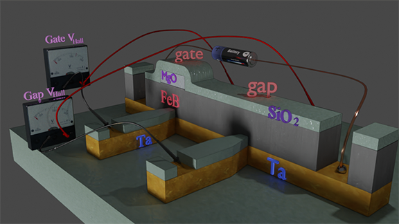
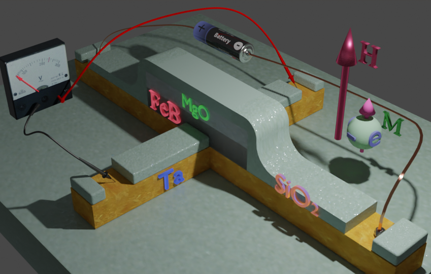
| Magnetic properties of nanomagnet (FeB, shown in grey) are changed when a gate voltage is applied at a metal- isolator interface at the top of the nanomagnet. The source battery provides the bias current through the metallic nanowire and the nanomagnet. The voltmeter measured the Hall voltage, which is created perpendicularly to the bias current. The gate voltage is applied between the top of nanomagnet and the nanowire. Because of thick (~ 10 nm) gate isolator (MgO), the gate voltage does not induce any electrical current. The gate modulation does not change the temperature of the nanomagnet. It is the main merit of the modulation of the magnetic properties of nanomagnet by a gate voltage. The effect, which describes the dependence of the magnetic properties on the gate voltage, is called the Voltage- Controlled Magnetic Anisotropy (VCMA). See details here. | ||||||
Modulation by bias current |
||||||
 |
||||||
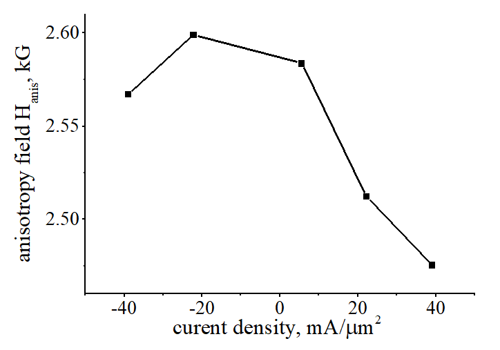
| Magnetic properties of nanomagnet are changed when the value of bias is changed. The source battery provides the bias current through the metallic nanowire and the nanomagnet. The voltmeter measured the Hall voltage, which is created perpendicularly to the bias current. Since the used current density is relatively large ~ 50 mA/um2 (otherwise the Hall voltage is to small to detect), the temperature of the nanomagnet is changed when the magnitude of the current change. Additionally, the magnetic properties of the nanomagnet depend on the polarity of the current. This effect is called Spin- Orbit Torque (SOT). (See details here) | ||||||
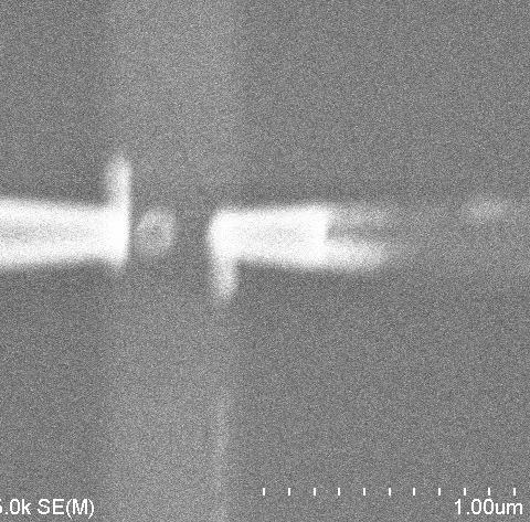
| Images made by Scanning Electron microscope SEM) of fabricated devices | ||||||
|
||||||
| click on image to enlarge it |
(a) SOT
(b) VCMA
(a) SOT
(b) VCMA
(a) SOT
(b) VCMA
(a) SOT
(b) VCMA
(a) SOT
(b) VCMA
(a) SOT
(b) VCMA
(a) SOT
(b) VCMA
(a) SOT
(b) VCMA
(a) SOT
(b) VCMA
(a) SOT
(b) VCMA
(a) SOT
(b) VCMA
![]() .........
......... ![]()
newest:
June 2022 ![]() nanomagnet2022.06.12.zip
nanomagnet2022.06.12.zip ![]()
old
January 2022 ![]() nanomagnet2022.01.10.zip
nanomagnet2022.01.10.zip ![]()
July 2021 ![]() 2021.07.01.zip
2021.07.01.zip ![]()
April 2021 ![]() data nanomagnet 2021.03.zip
data nanomagnet 2021.03.zip ![]()

![]() click on image to enlarge it
click on image to enlarge it
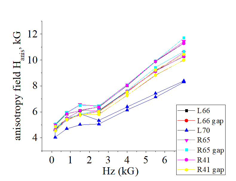
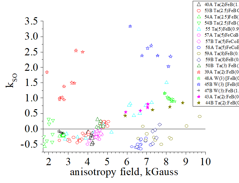
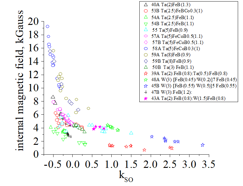
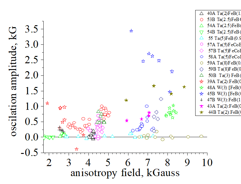
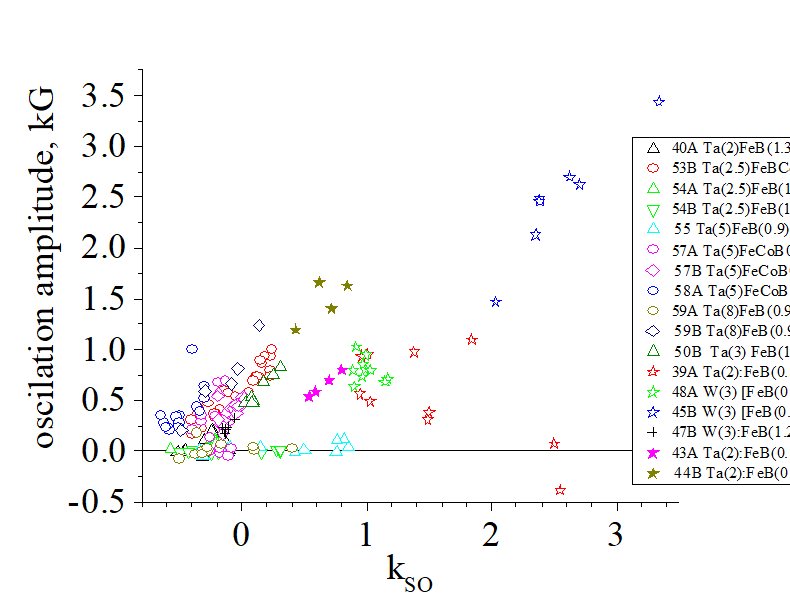
| Coefficient of spin-orbit interaction kSO vs. anisotropy field Hani | Internal magnetic field vs. coefficient of spin-orbit interaction kSO | |
|---|---|---|
 |
 |
|
| For a single-layer or double-layer nanomagnets, the slope is positive. For a multilayer nanomagnets (green and blue stars), the slope is negative. | The effective magnetic field decrease with the increase of kSO. It is because the interface smoothness, which leads to a larger HSO and kSO, also leads to a larger demagnetization field. |
| Amplitude of oscillation of Hani vs. anisotropy field Hani | Amplitude of oscillation of Hani vs. coefficient of spin-orbit interaction kSO | Amplitude of oscillation of Hani. vs. coefficient of spin-orbit interaction kSO |
|---|---|---|
 |
 |
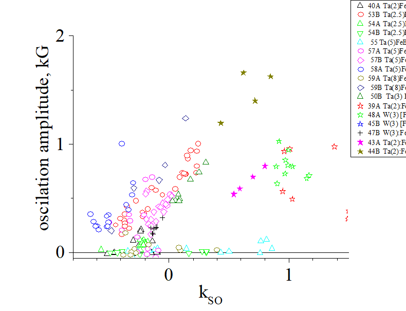 |
| Oscillation amplitude and kSO simultaneously become larger. It is because they both are originated by the interface. When the contribution of the interface becomes larger and the contribution of the bulk becomes smaller, both the oscillation amplitude and kSO become larger. | the same as the left figure, but with a different scale. |
 All measurement method have been developed by me in 2018-2020. The features of all methods are a high- repeatability, high-reproducibility and very high measurement precision. I do my best to avoid and eliminate any possible systematical error.
3 measurement methods to characterize magnetic and magneto- transport properties of a nanomagnet |
||||||
|
||||||
| All three measurements were developed and optimized in 2019-2020. The features of all methods are a high- repeatability, high-reproducibility and very high measurement precision. | ||||||
| Click on image to enlarge it |
(high repeatability, high reproducibility)![]() I have checked re measured some random samples after ~one year after their first measurement. All measurements gave exactly same results with the measurement precision.
I have checked re measured some random samples after ~one year after their first measurement. All measurements gave exactly same results with the measurement precision.
(high measurement precision)![]() I have achieved a very high measurement precision for all my methods. E.g. I can measure the coercive field with precision of 0.1 Oe (See here) , which is very hard to achieve by any other known measurement methods. I am constantly improving my measurement setup in order to reduce measurement noise and therefore to improve the measurement precision.
I have achieved a very high measurement precision for all my methods. E.g. I can measure the coercive field with precision of 0.1 Oe (See here) , which is very hard to achieve by any other known measurement methods. I am constantly improving my measurement setup in order to reduce measurement noise and therefore to improve the measurement precision.
(free of a systematic error)![]() To avoid a systematical error is the major challenge for any high- precision measurement method. In order to avoid a systematical error, I time- to time verify a measurement by several independent measurement method. Achievement of the same value of the parameter measured by independent methods is a good indication that there is no systematical error.
To avoid a systematical error is the major challenge for any high- precision measurement method. In order to avoid a systematical error, I time- to time verify a measurement by several independent measurement method. Achievement of the same value of the parameter measured by independent methods is a good indication that there is no systematical error.
(measurement method 1): Fit |
||||||
|
||||||
|---|---|---|---|---|---|---|
| Simultaneous fit for 0, 1st and 2nd derivatives are perfect. | ||||||
| There are always some oscillations for 2nd derivative. As 2020.04, their origin is unknown. | ||||||
| Sample Volt 54B free 28 | ||||||
| Click on image to enlarge it |
![]() The method 1 is very difficult to use (or even impossible to use) for a larger- size nanomagnet or a continuous film due to their domain structure.
The method 1 is very difficult to use (or even impossible to use) for a larger- size nanomagnet or a continuous film due to their domain structure.
A. Yes.
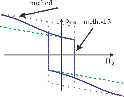
(indication 1 for existence of static domains): there are sharp peaks for 1st and 2nd derivatives
(indication 2 for existence of static domains): the fitting is impossible
(indication 3 for existence of static domains): red,green, blue and light- blue lines of Fig.11 do not coincide
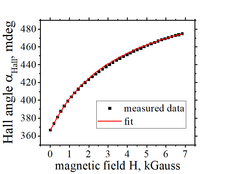
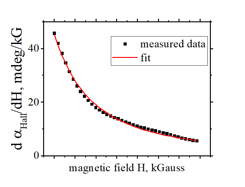
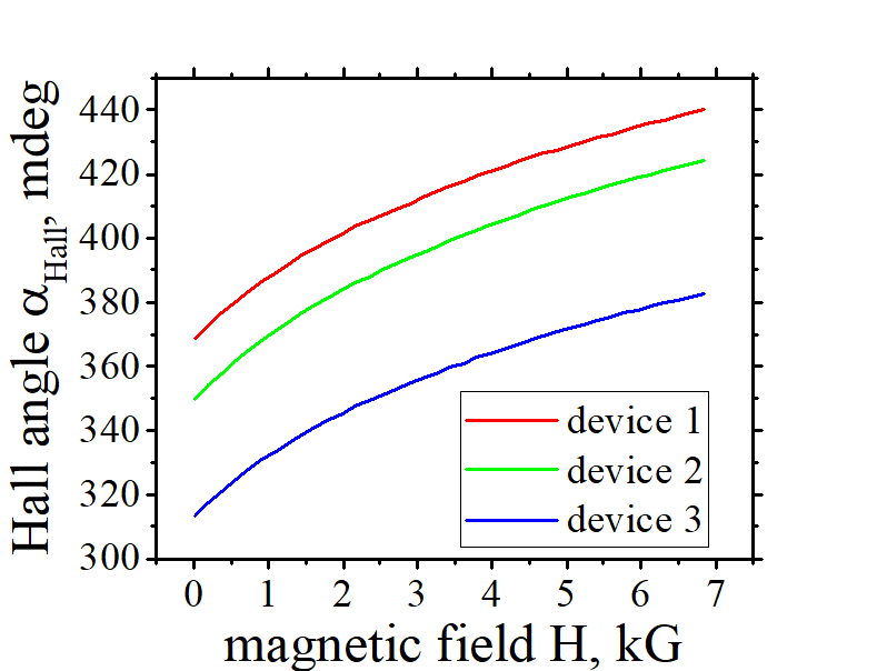
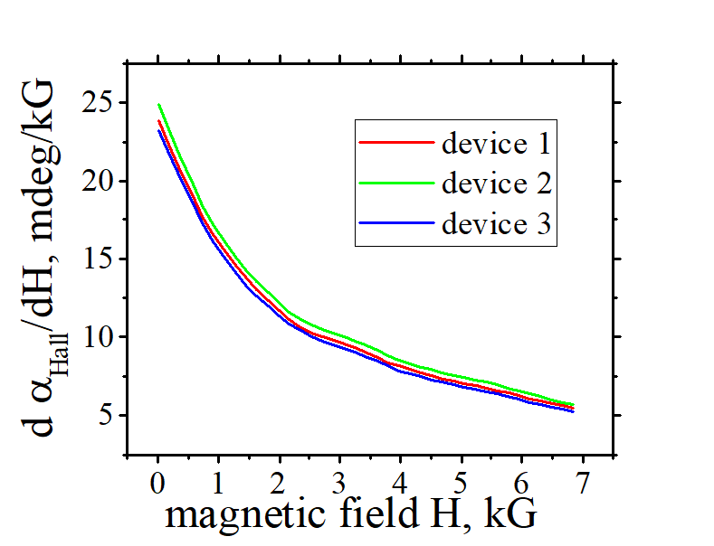
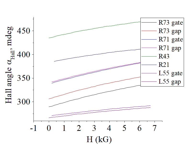
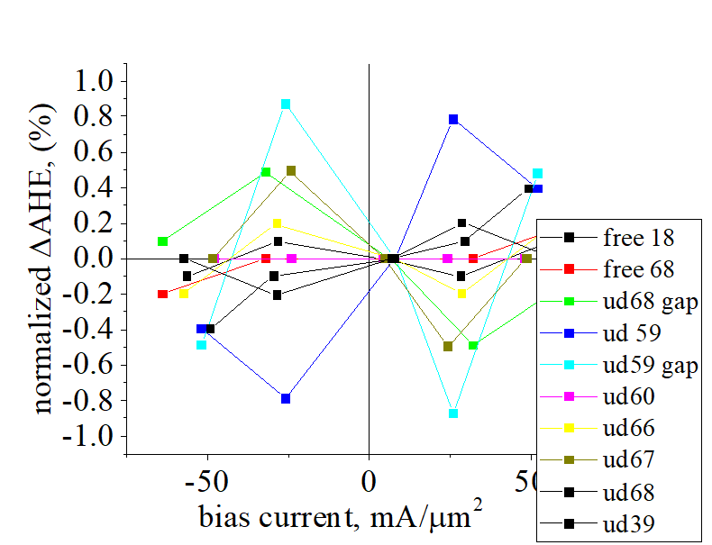
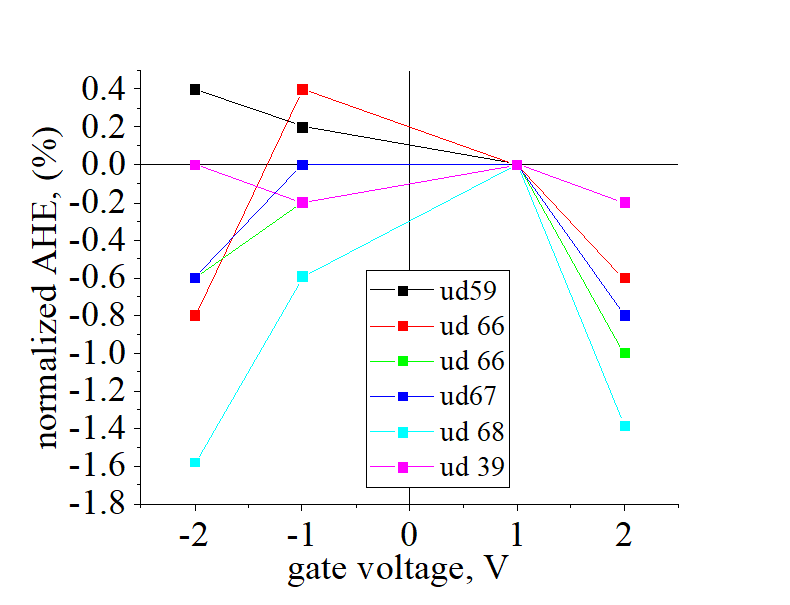
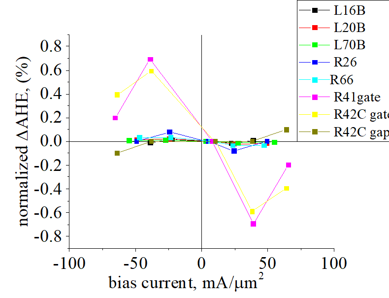
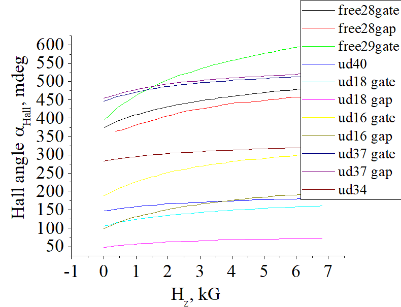
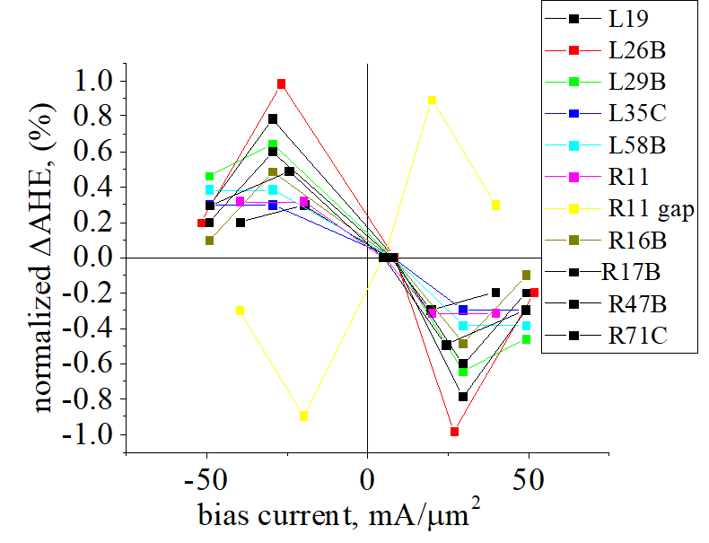
(measurement method 1): Measurement of AHE and ISHE contributions. Sample- to- sample dependence |
|||||||||
|
|||||||||
|---|---|---|---|---|---|---|---|---|---|
| The measurement clearly indicate that AHE change substantially and ISHE nearly does not change from a device to device | |||||||||
| Note: some samples show a substantial device- to- device difference of both αAHE and αISHE. . See below detailed measurements for each sample | |||||||||
| Sample Volt 54B | |||||||||
| Click on image to enlarge it |
(note) ![]() Often the difference of the αHall between different nanomagnets of the same sample is a constant offset of αHall without a change (or with a very small change) of its 1st and 2nd derivatives (E.g. sample Volt54). It indicates that there is a difference of magnitude of AHE between samples, but the variation of the ISHE and spin polarization sp of the electron gas is weak from a nanomagnet to nanomagnet .
Often the difference of the αHall between different nanomagnets of the same sample is a constant offset of αHall without a change (or with a very small change) of its 1st and 2nd derivatives (E.g. sample Volt54). It indicates that there is a difference of magnitude of AHE between samples, but the variation of the ISHE and spin polarization sp of the electron gas is weak from a nanomagnet to nanomagnet .
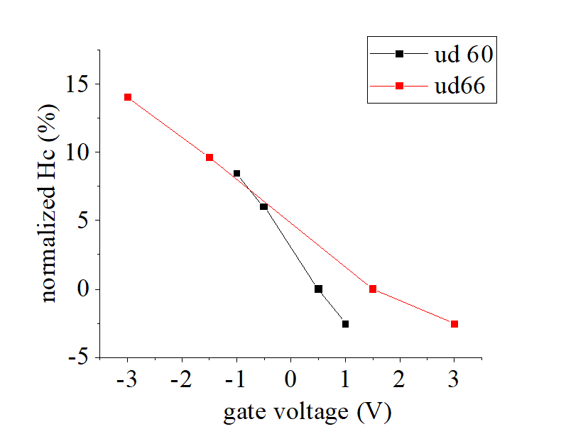
(measurement method 1): Measurement of AHE and ISHE contributions. Current dependence |
|||||||||
|
|||||||||
|---|---|---|---|---|---|---|---|---|---|
| The measurement clearly indicate that the current change substantially AHE, but it nearly does not influence ISHE | |||||||||
| Note: some samples show a substantial- current dependence of both αAHE and αISHE. See below detailed measurements for each sample | |||||||||
| Sample Volt 54B free 28 | |||||||||
| Click on image to enlarge it |
(note):![]() For the most of sample (E.g. Sample Volt 54B free 28), a different gate voltage or bias current makes a constant change of αHall without a change (or with a very small change) of 1st and 2nd derivatives. It indicates that the gate voltage or bias current mainly influence the AHE and only weakly influence the ISHE and spin polarization sp of the electron gas.
For the most of sample (E.g. Sample Volt 54B free 28), a different gate voltage or bias current makes a constant change of αHall without a change (or with a very small change) of 1st and 2nd derivatives. It indicates that the gate voltage or bias current mainly influence the AHE and only weakly influence the ISHE and spin polarization sp of the electron gas.
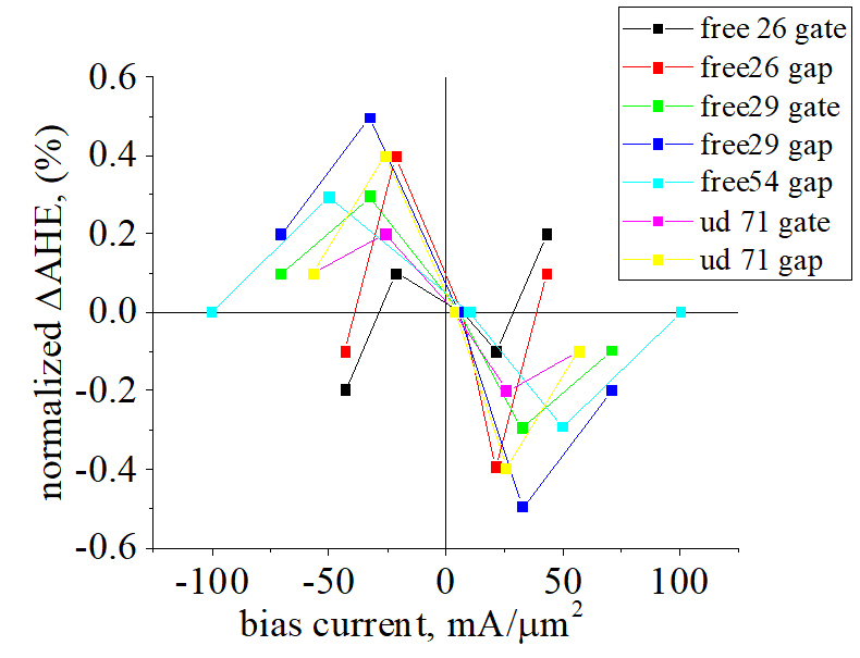
(measurement method 1): Separation and calculation of AHE and ISHE contributions. Current dependence |
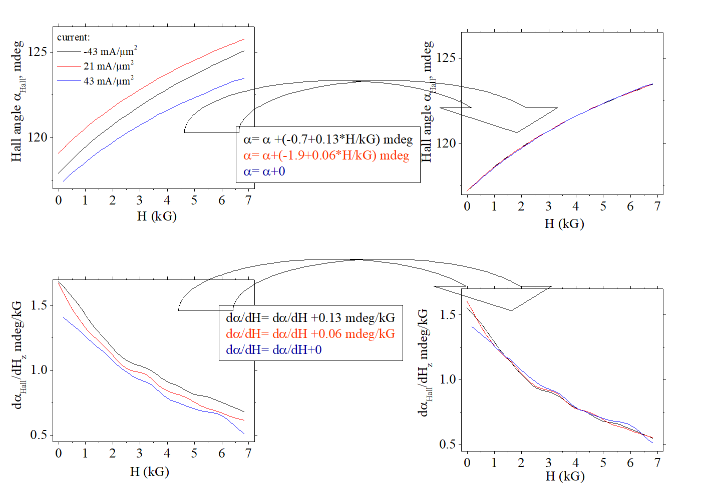 |
| (left side: Measured data) : Both αHall and dαHall /dHz depend on the current |
| (right side: data fitted to each other) : (step 1) (right- bottom graph): fitting of 1st derivative dαHall /dHz measured at different currents into one single line (step 2) (right- top graph):. Fitting of measured αHall at different currents into one single line. After two steps all lines fit perfectly in one single line.. |
| Note: 2nd derivative behaves similar to 1st derivative |
|
| When current j is change from 43 to 23 mA/ μm2, AHE change is ΔαAHE =-1.9 mdeg and change of derivative ISHE Δ(dαISHE/dH)= 0.06 mdeg/kG |
| When current j is change from +43 to -43 mA/ μm2, AHE change is ΔαAHE = -0.7 mdeg and change of derivative ISHE Δ(dαISHE/dH)= 0.13 mdeg/kG |
| Sample: Volt57B L20 |
| Fig.31. Click on image to enlarge it |
Due to the an ambiguity of the fitting αHall (See here), it is difficult to calculate the absolute values of the magnitude αAHE of Anomalous Hall effect (AHE), the magnitude αISHE of Inverse Spin Hall effect (ISHE) and the spin polarization sp of the electron gas. However, it is possible to measure their relative changes ![]() under a different gate voltage or bias current or a changes from sample to sample
under a different gate voltage or bias current or a changes from sample to sample
Figure 31 shows measured data of sample, in which both αHall and its 1st derivative change for a different bias current. The measured data are shown at right side of figure. It is clear that current dependences for αHall and its 1st derivative are different and independent.
(note) the current dependence of the 2nd derivative (not shown) is similar to the current dependence of the 1st derivative
It can be assumed that the bias current only affects αAHE and αISHE other parameters, which may influence αHall , remain unchanged.
(step 1). Since αAHE is a constant vs H, the 1st derivative (and 2nd derivative) is proportional to αISHE and is not influenced by αAHE. Lines of left- bottom graph are clearly parallel and their difference is a constant. Adding a constant to 1st derivative, it is possible to fit all lines, which corresponds to 1st derivative at a different current, to one single line (See bottom right graph). It gives the difference of magnitude ΔαISHE of ISHE at a different currents
(step 2) After correction of αHall for , the lines in top- left graphs becomes parallel and and their difference becomes a constant. Adding corresponded constant to each line, it is possible to fit all lines to one single line (See top- right graph). It gives the difference of magnitude ΔαAHE of AHE at different currents
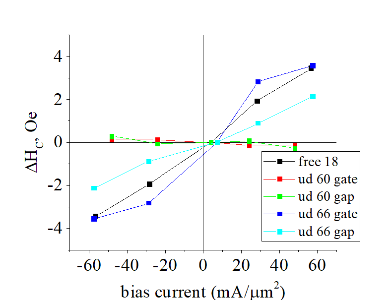
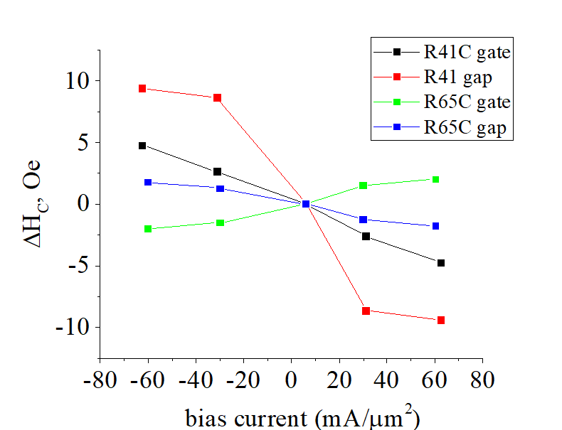
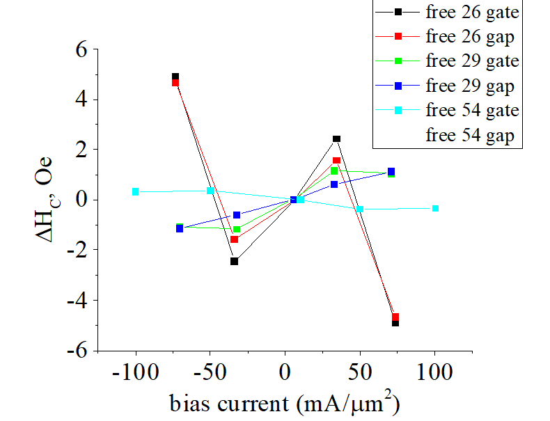
Measurement of anisotropy field, strength of perpendicular magnetic anisotropy (PMA), " field- like torque" and "damp- like torque"
| Method 2: Measurement of PMA strength |
|---|
 |
| (measurement the strength of PMA) |
| ( Hani as a measure of PMA energy) |
| (additional measurement: measurement of SOT effect) |
Note. I have developed this measurement method in 2019-2020 |
| click on image to enlarge it |
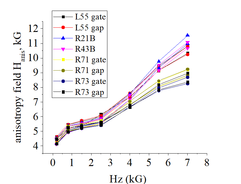
(measurement method 2): Measurement of Hanis, PMA strength, " field- like torque" and "damp- like torque |
|||
|
|||
|---|---|---|---|
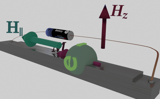
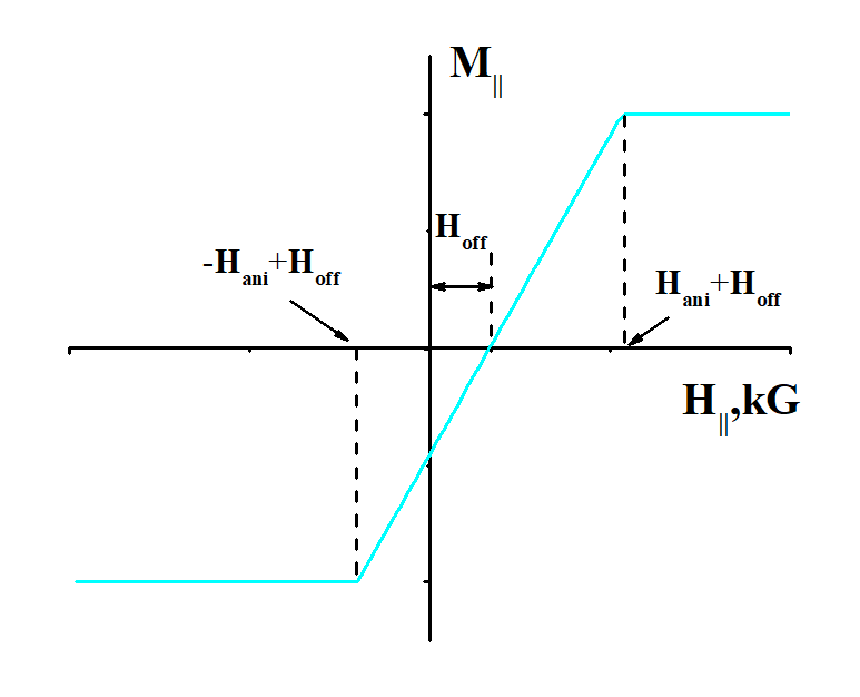
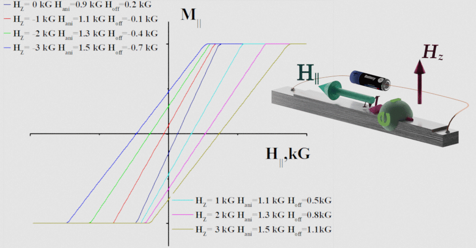
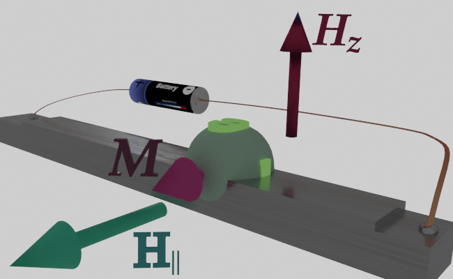
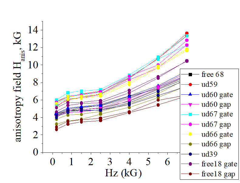
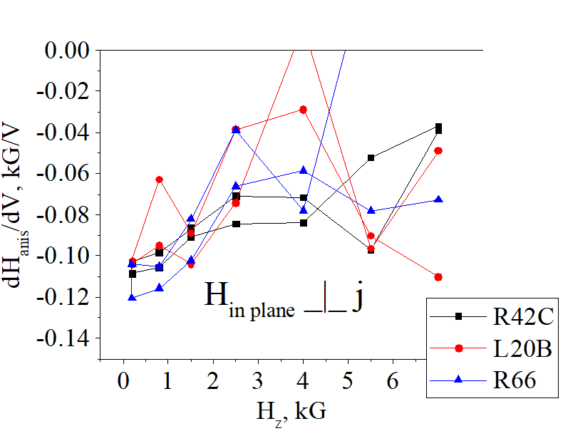
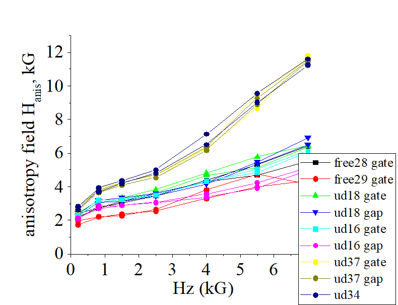
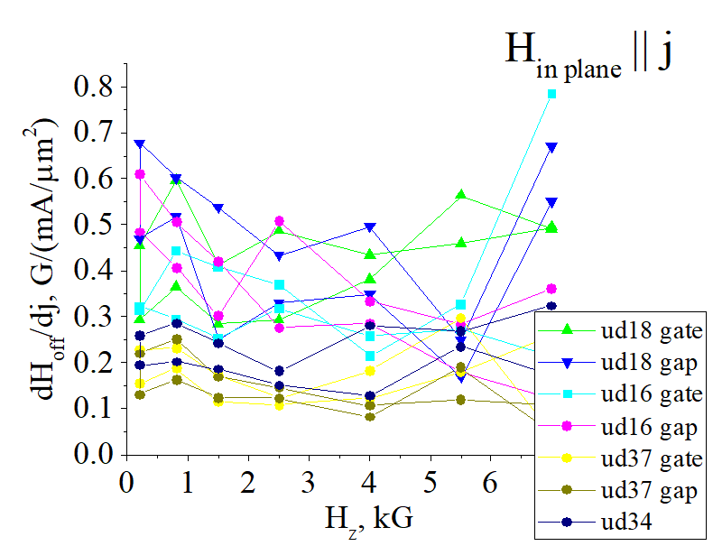
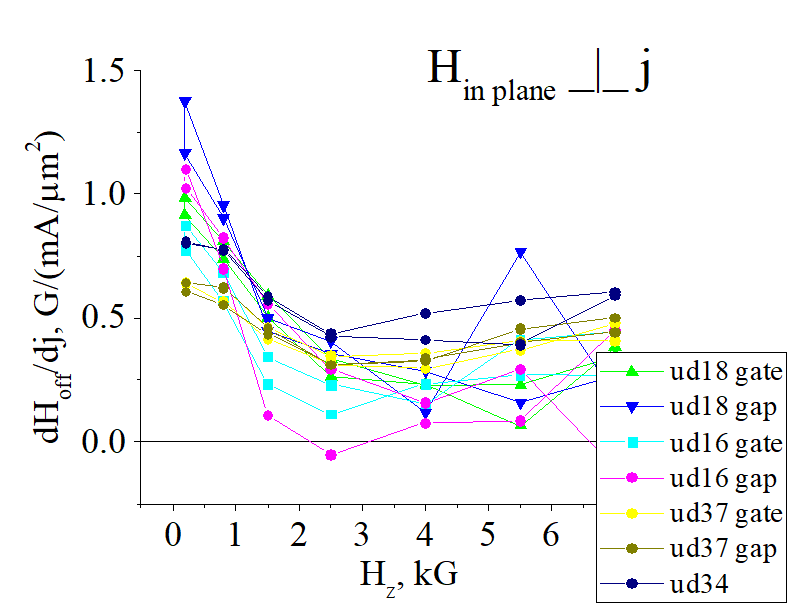
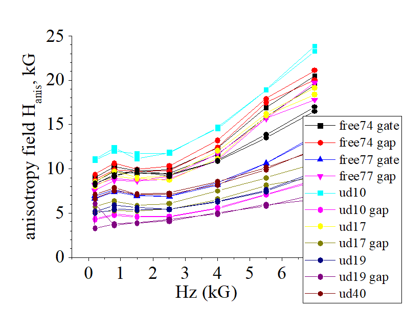
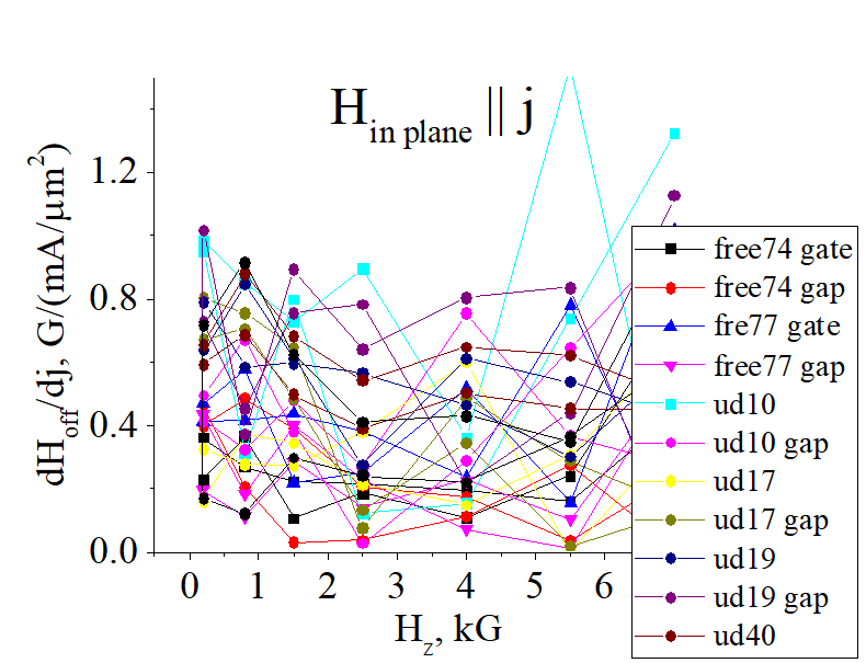
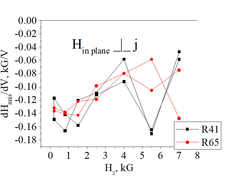
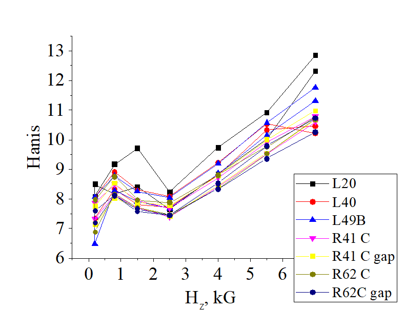
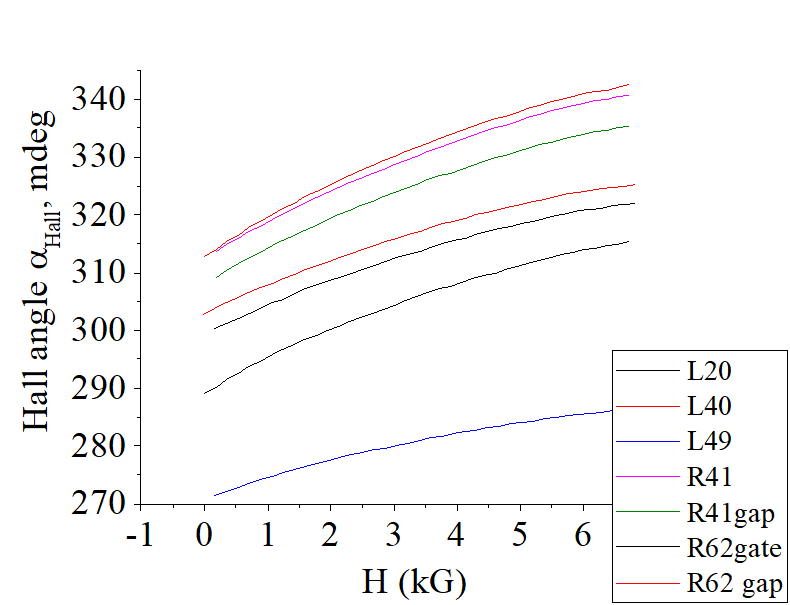
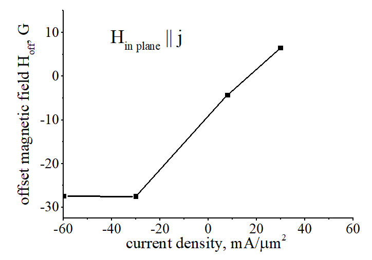
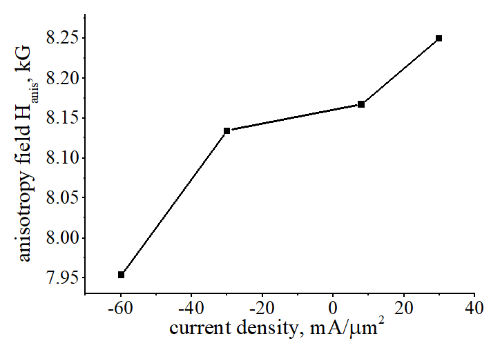
| External magnetic field H|| is applied in-plane and perpendicularly to the magnetization (along the hard axis). As a result, the magnetization turns towards the magnetic field. The magnetic field, at which the magnetization turns completely in-plane, is called the anisotropy field Hanis . The Hanis is a measure of the strength of the perpendicular magnetic anisotropy (PMA). In order to characterize the features of the PMA, an additional field Hz is applied perpendicularly to the film | |||
| (what is measured) |
|||
| (which parameters are evaluated) |
|||
Note. I have developed this measurement method in 2019-2020 |
|||
| Click on image to enlarge it |
(main idea): ![]() In-plane component of magnetization M|| is measured under an in-plane external magnetic field H||. In absence of the magnetization M is perpendicular to the plane. Under H|| the M turns towards H|| until its direction is fully in-plane. The stronger the PMA is, the large H|| is required to turn M fully in- plane.
In-plane component of magnetization M|| is measured under an in-plane external magnetic field H||. In absence of the magnetization M is perpendicular to the plane. Under H|| the M turns towards H|| until its direction is fully in-plane. The stronger the PMA is, the large H|| is required to turn M fully in- plane.
(How does it work) An external magnetic field (in- plane field H||) i applied perpendicularly to the stable magnetization (easy axis) of the nanomagnet (perpendicular- to plane). Even though the magnetization is turning towards and away from its the equilibrium direction (easy axis), it resists against the turning. Method 3 measures the strength of this resistance and therefore the magnetic energy, which contains in the nanomagnet. An. additional magnetic field Hz is applied to enhance the resistance against the turning and therefore it more clarifies the magnetic features of the nanomagnet.
![]() (Which parameters are measured)
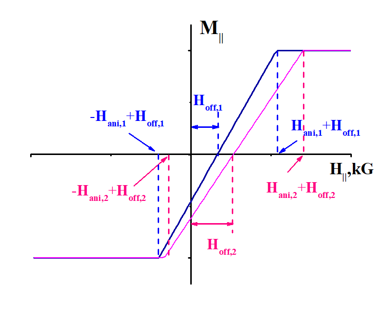
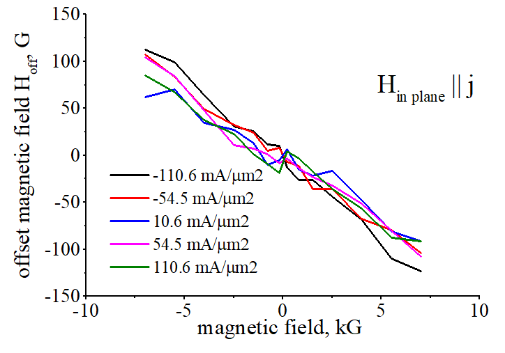
(Which parameters are measured)![]() Two parameters are measured: (parameter 1) Angle of line M|| vs H||, which gives the anisotropy field Hani The Haniis the field at which the line crosses the x-axis and therefore the magnetization is aligned fully in- plane. (parameter 2). The offset magnetic field Hoff, . The Hoff is the magnetic field, for which the line is shifted from the axis origin.
Two parameters are measured: (parameter 1) Angle of line M|| vs H||, which gives the anisotropy field Hani The Haniis the field at which the line crosses the x-axis and therefore the magnetization is aligned fully in- plane. (parameter 2). The offset magnetic field Hoff, . The Hoff is the magnetic field, for which the line is shifted from the axis origin.
(measurement method 2): Measurement of Hanis, PMA strength, " field- like torque" and "damp- like torque |
|||||||||
|
|||||||||
| Click on image to enlarge it |
 (What is new in the proposed measuremengt method)
![]() Two
Two
(old measurement method): in-plane magnetization M|| is measured under scan of H|| without any perpendicular field Hz
(new proposed measurement method): in-plane magnetization M|| is measured under scan of H|| at a different perpendicular field Hz
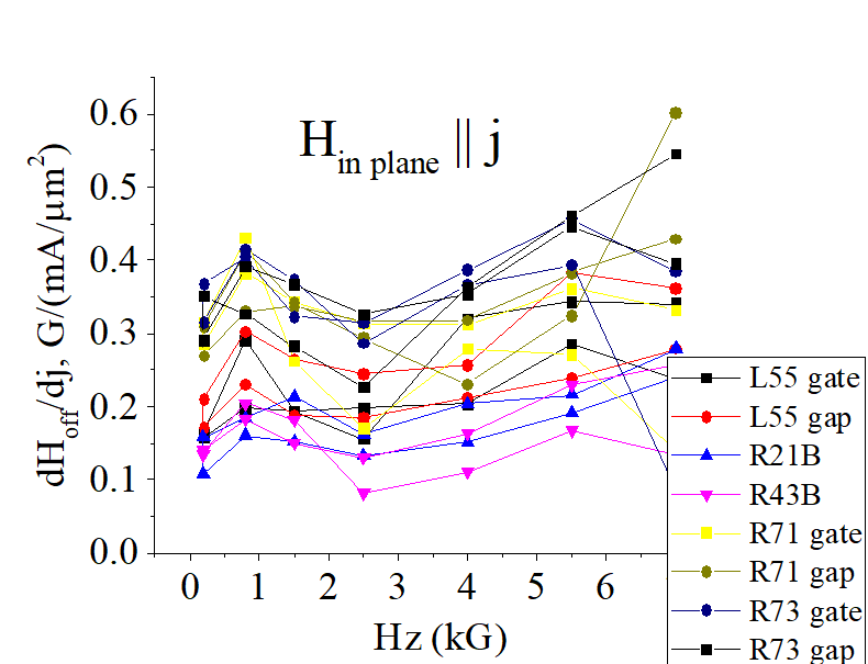
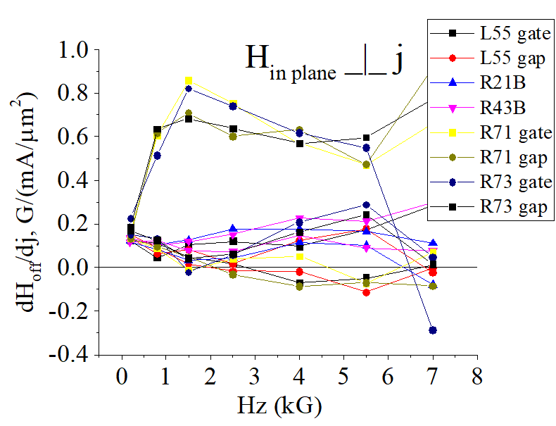
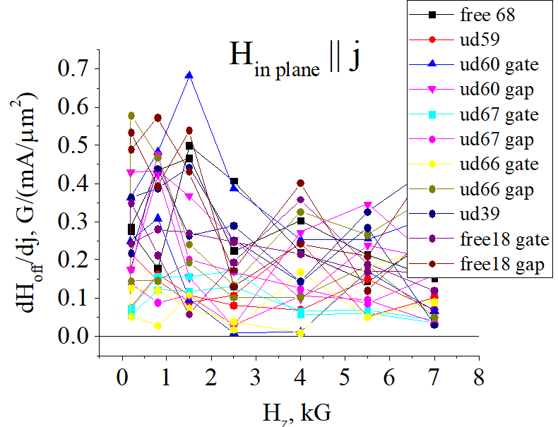
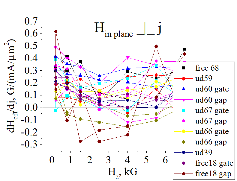
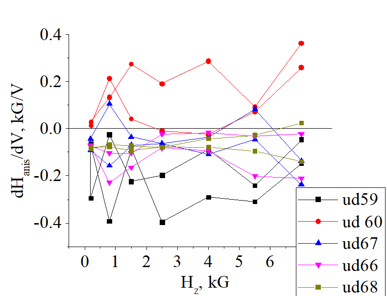
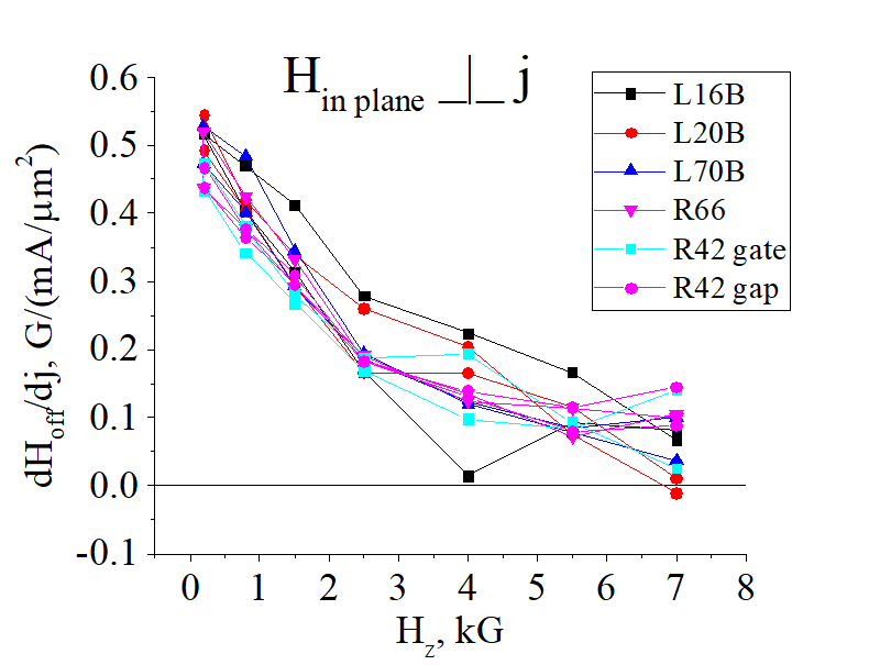
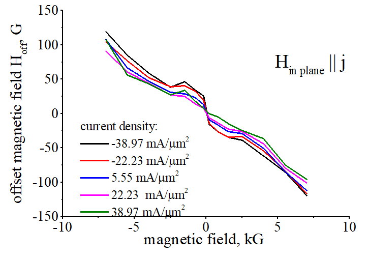
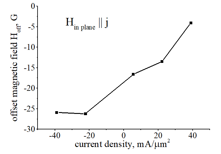
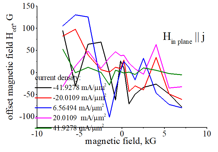
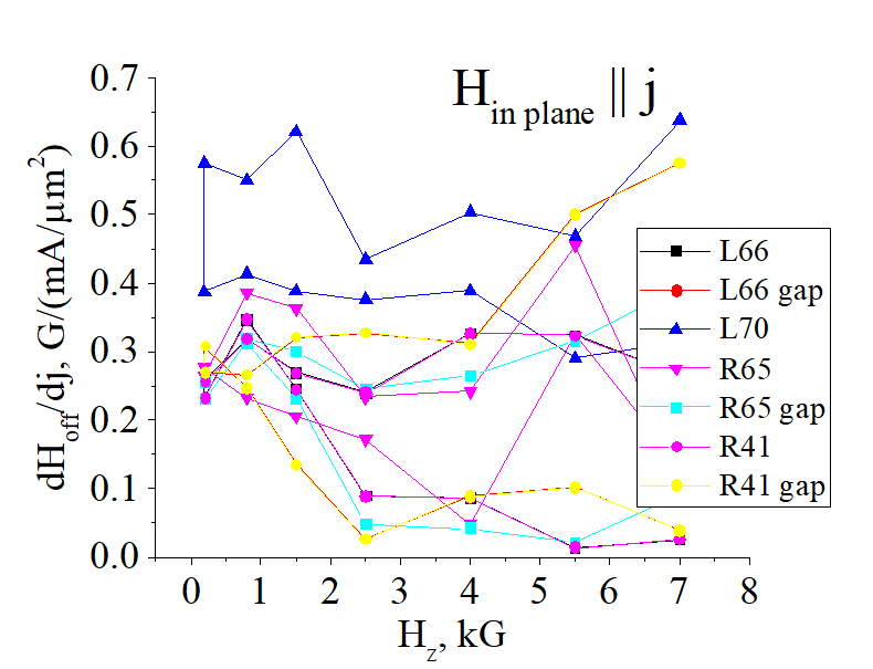
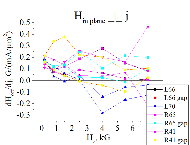
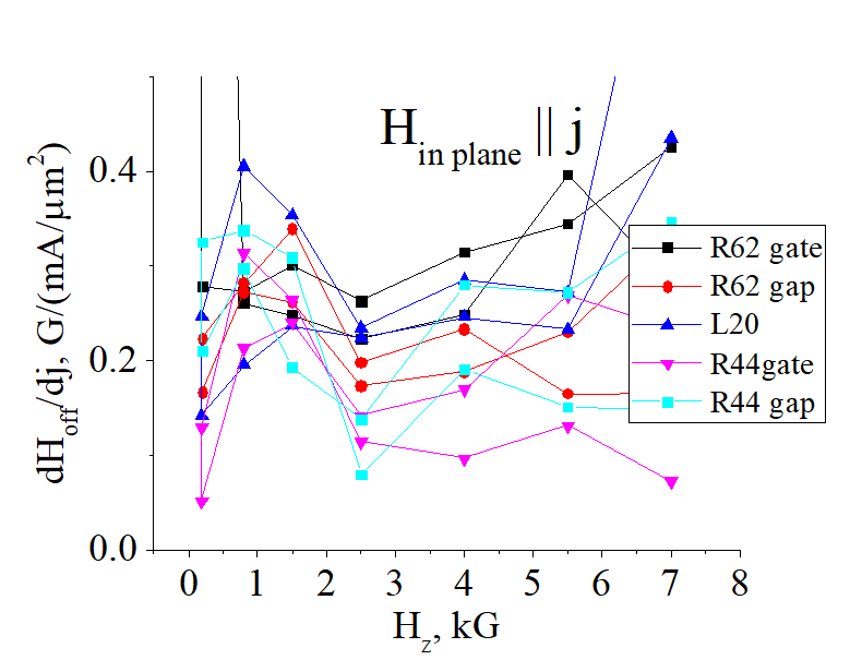
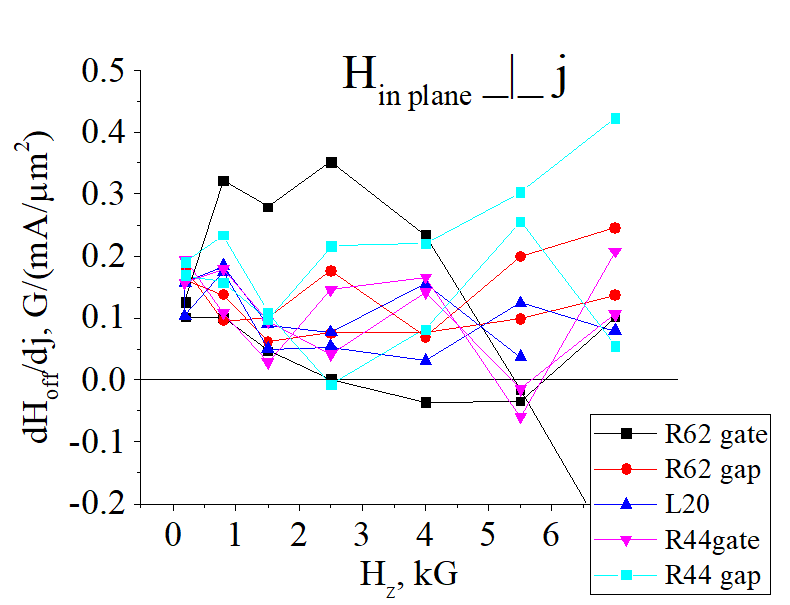
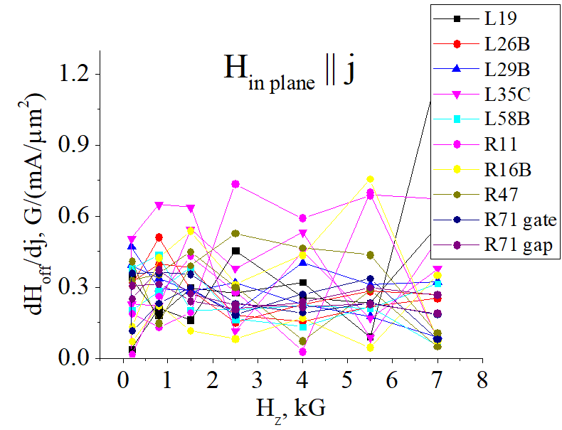
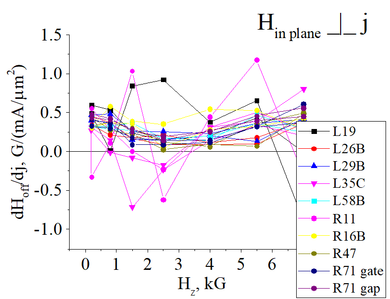
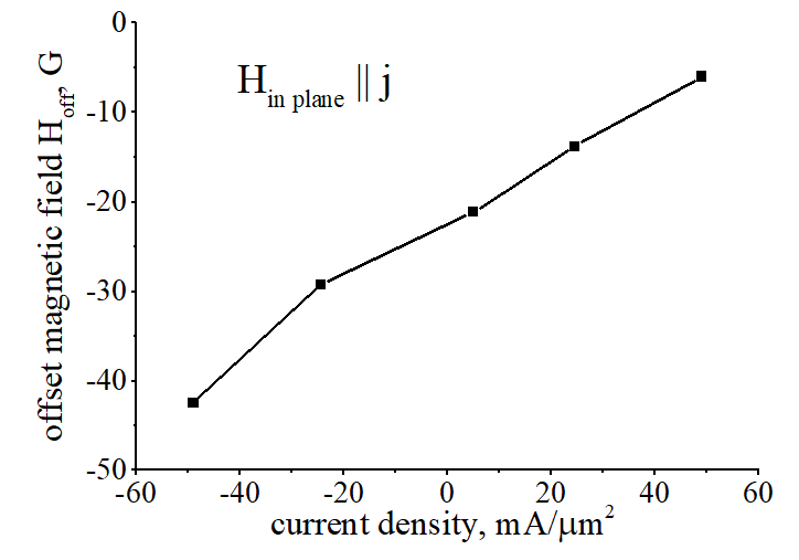
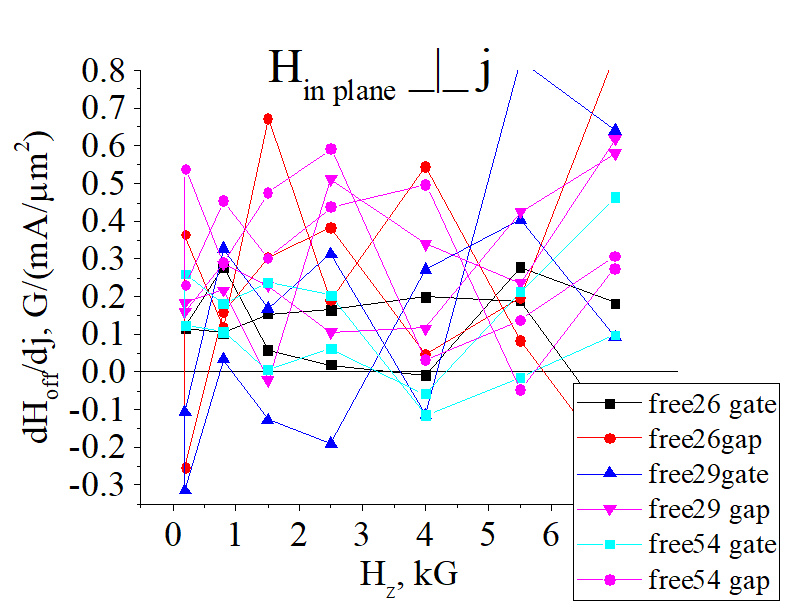
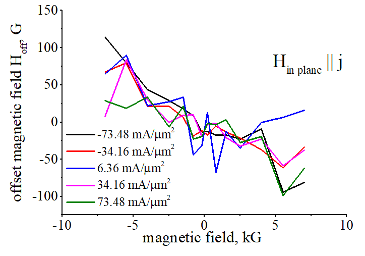
(measurement method 2): Offset magnetic field Hoff vs perpendicular magnetic field Hz |
||||||||||
|
||||||||||
| Click on image to enlarge it |
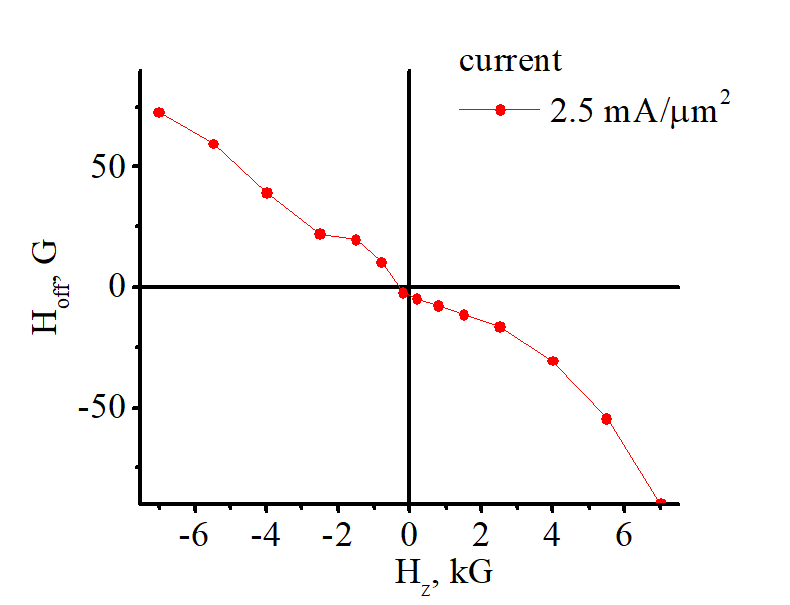
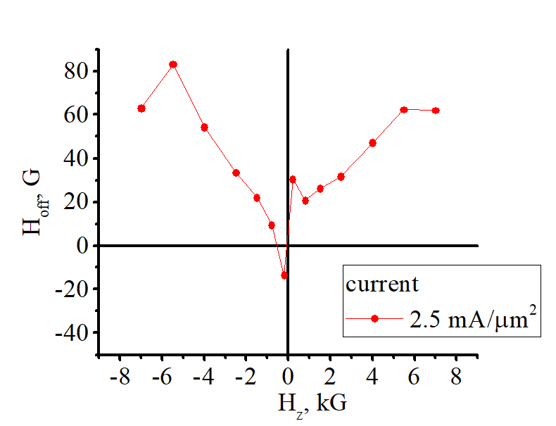
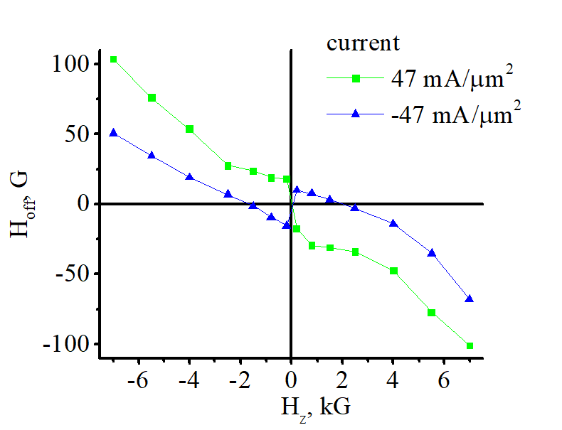
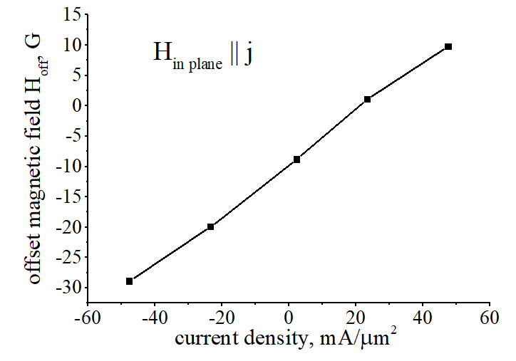
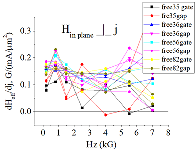
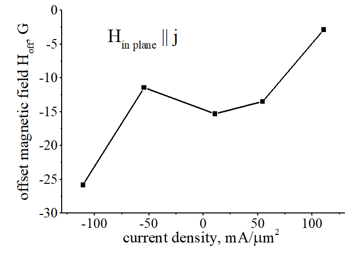
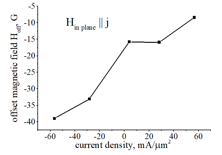
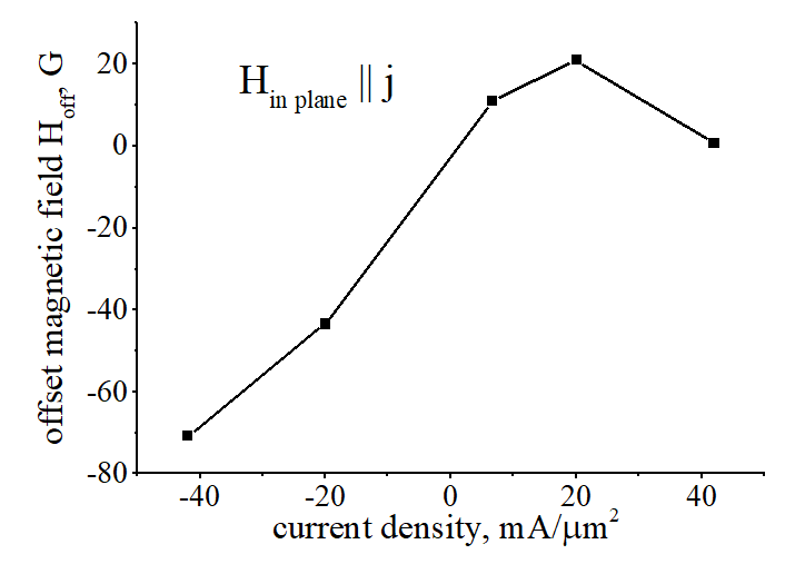
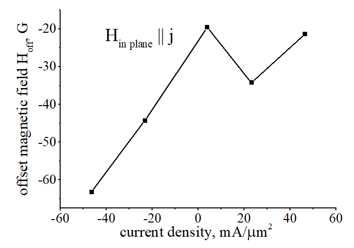
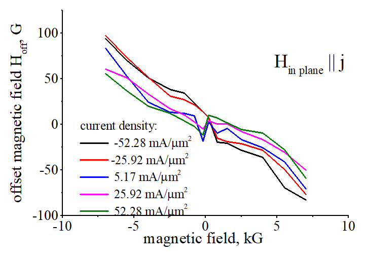
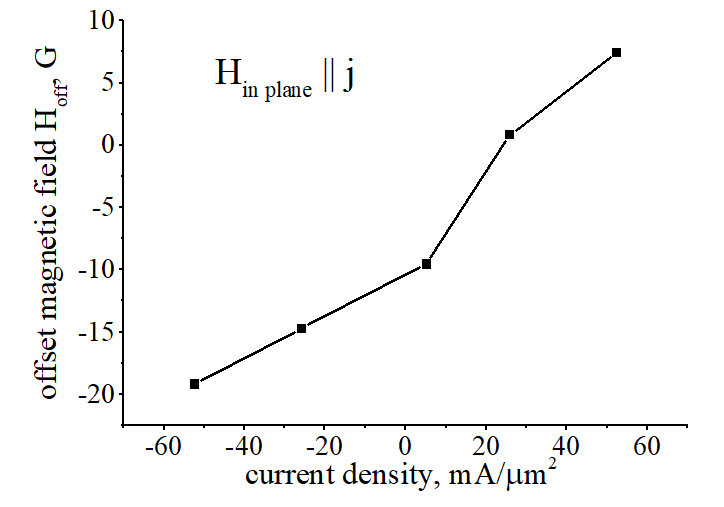
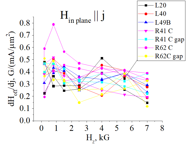
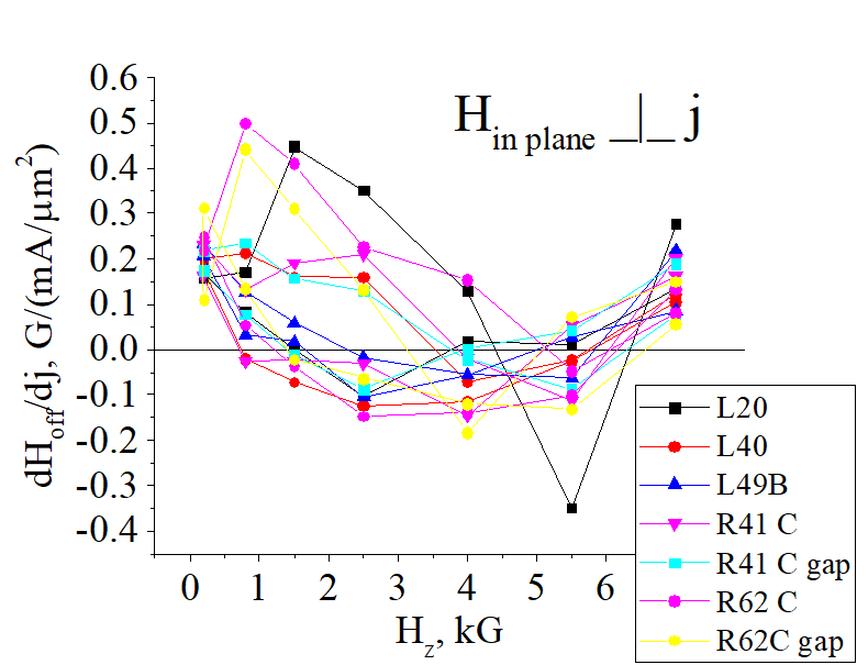
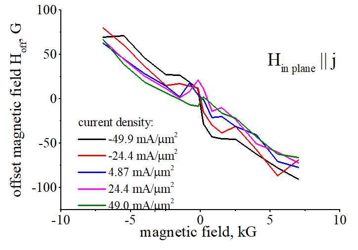
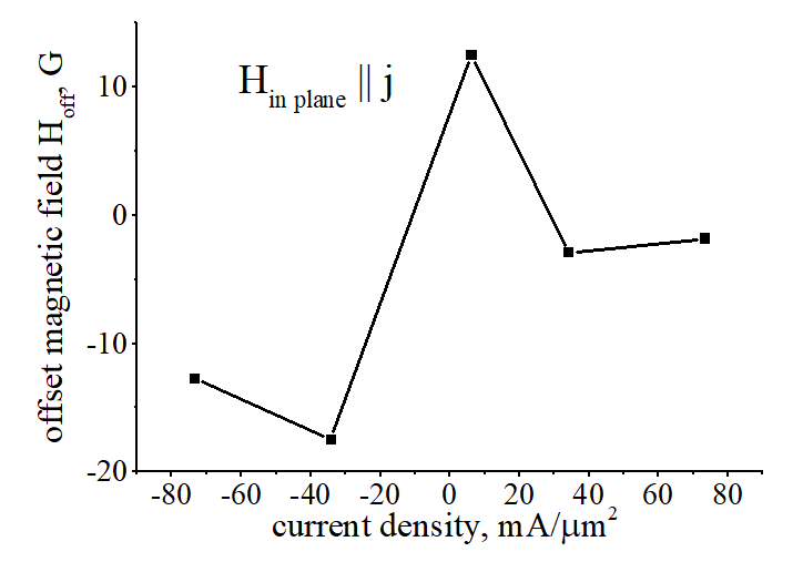
(fact 1) ![]() There is in- plane magnetic field in ferromagnetic nanomagnet, which induced by PMA effect at boundaries of the nanomagnet.
There is in- plane magnetic field in ferromagnetic nanomagnet, which induced by PMA effect at boundaries of the nanomagnet.![]()
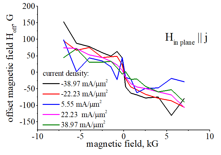
(fact 2) ![]() The magnitude and direction in- plane magnetic field Hoff increases and changes direction when an external magnetic field Hz is applied perpendicularly- to- plane of the nanomagnet
The magnitude and direction in- plane magnetic field Hoff increases and changes direction when an external magnetic field Hz is applied perpendicularly- to- plane of the nanomagnet ![]()
fact 3) ![]() The magnitude and direction of in- plane magnetic field Hoff are different for opposite polarities of the external magnetic field Hz It indicates
The magnitude and direction of in- plane magnetic field Hoff are different for opposite polarities of the external magnetic field Hz It indicates ![]()
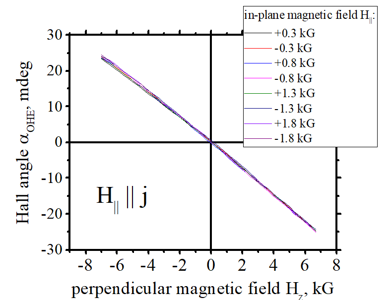
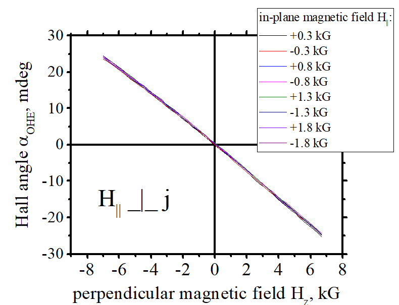
A. I have calibrated magnet with precision about 0.1 Oe by measuring the Hall effect in non-magnetic metal Ru (See below).
(measurement method 2): Offset magnetic field Hoff vs perpendicular magnetic field Hz |
||||||||
|
||||||||
| Click on image to enlarge it |
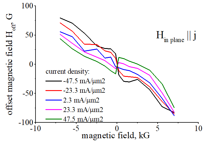
A magnetic field creates a torque on magnetic torque
(type 1 of magnetic field) ![]()
![]() "Field - like torque"
"Field - like torque"
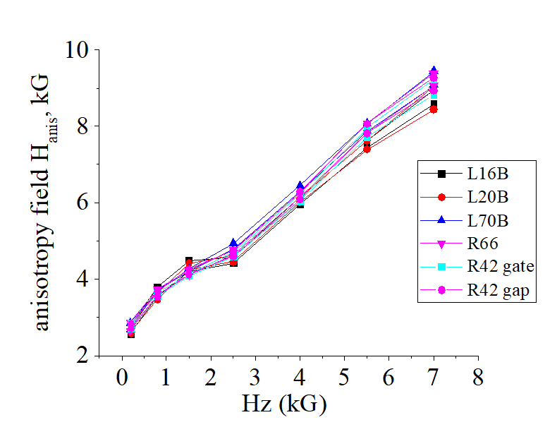
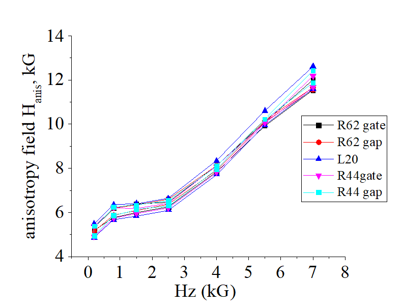
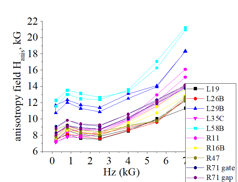
Measurement of anisotropy field Hani |
|||||||||
|
|||||||||
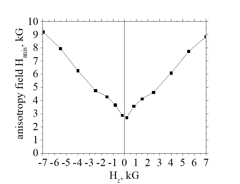
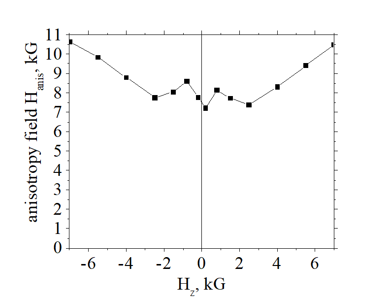
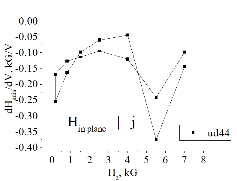
| Anisotropy field Hani for a nanomagnet is defined as the minimal point at Hz =0. | |||||||||
| The dependence diverse from a linear and contains some oscillation of an unknown origin in region |Hz|< 2kG | |||||||||
| anisotropy field is calculated from the slope of dependence M|| vs H||(See above) | |||||||||
| Click on image to enlarge it |
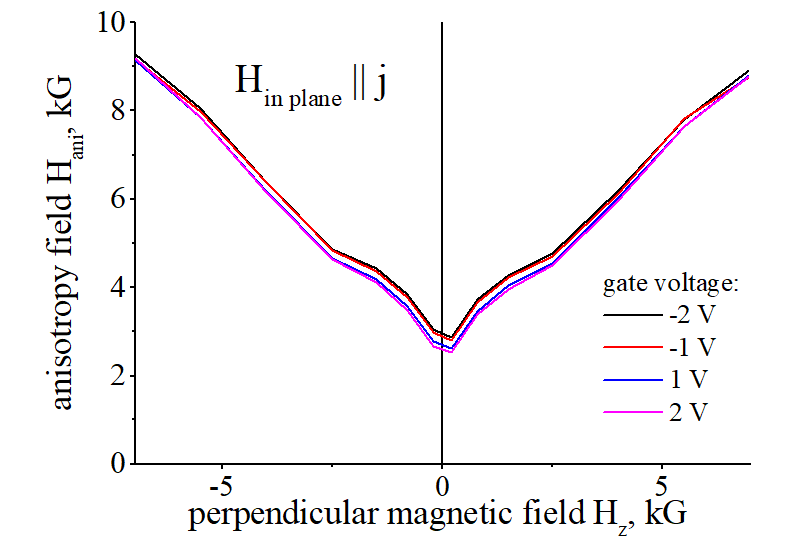
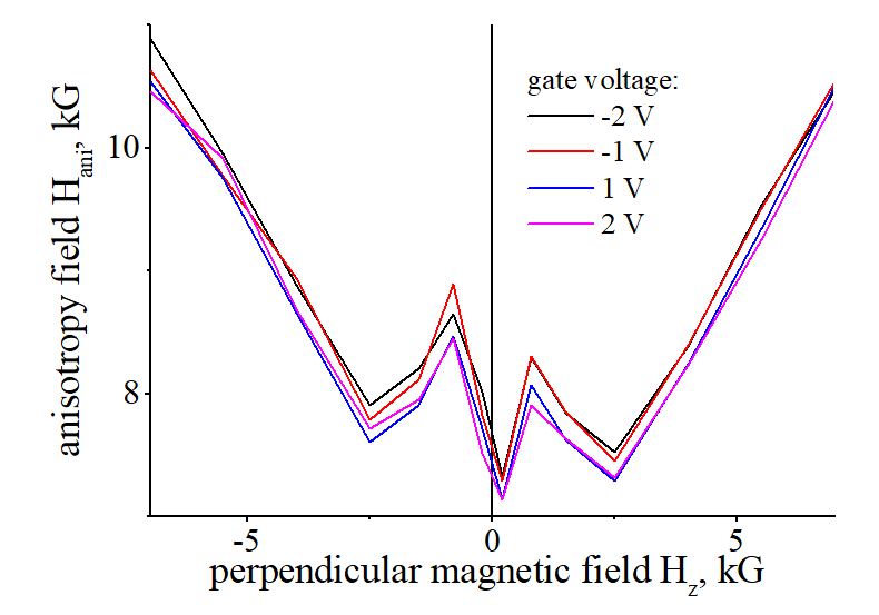
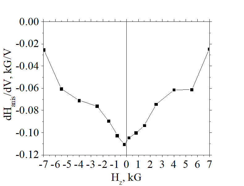
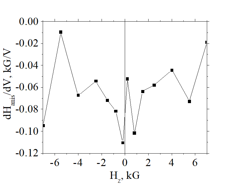
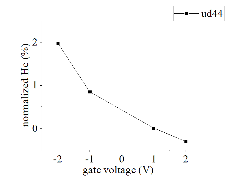
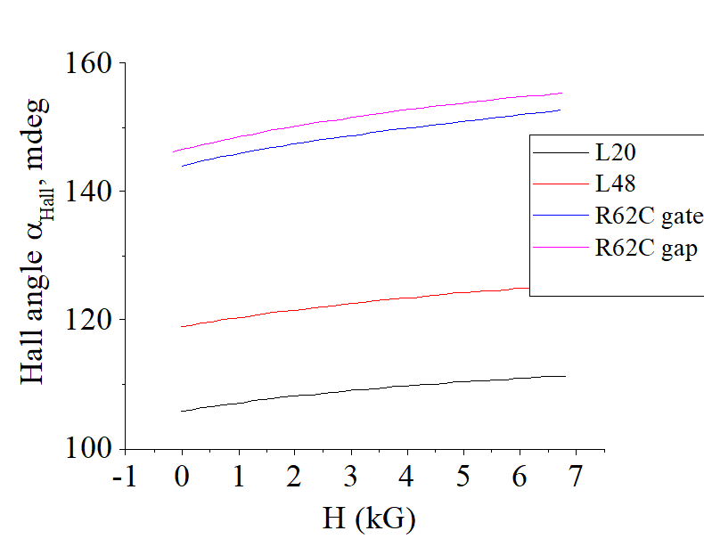
Measurement of anisotropy field Hani on gate voltage (VCMA effect) |
||||||||
|
||||||||
| Click on image to enlarge it |
(Verification experiment for magnetic alignment)): |
||||
|
||||
| Sample: Ref30 (Ru 25 nm). Rotation angle (dαOHE/dHz=-3.7 mdeg/kG) | ||||
| Click on image to enlarge it |
Content
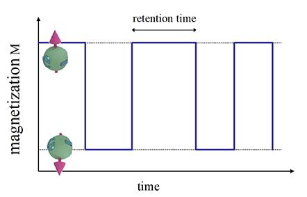
measurement of coercive field, retention time, size of nucleation domain and parameter delta
| Measurement method 3:measurement of parameters of thermally- activated switching |
|---|
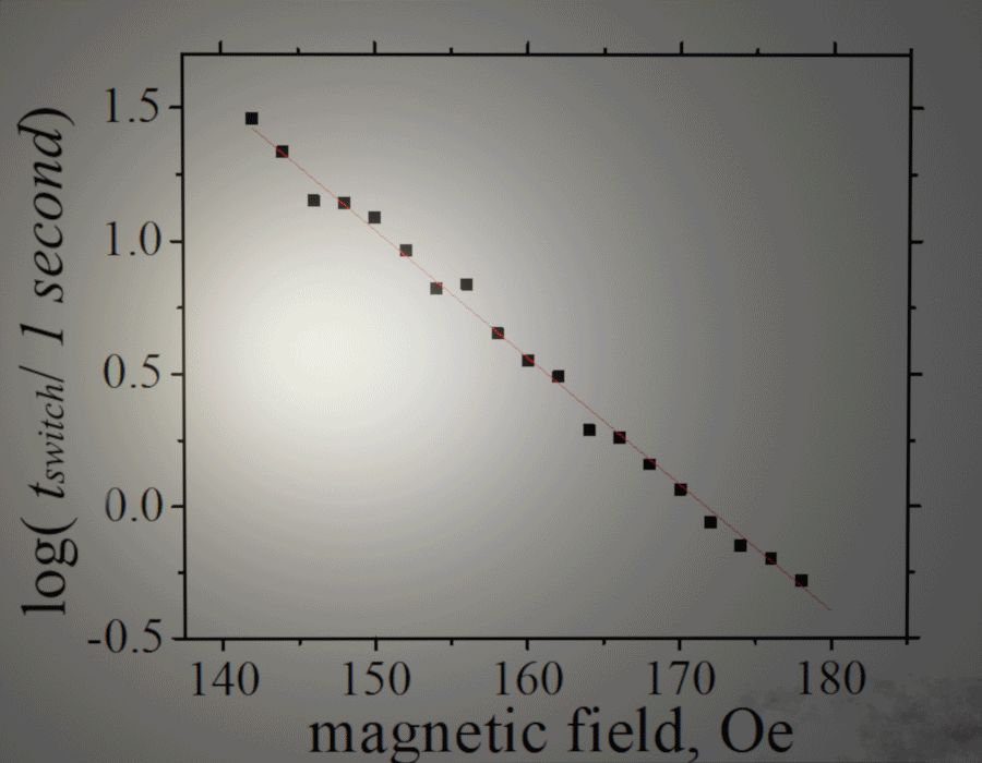 |
| (measurement method): |
| (thermally-activated switching): |
| (features of the method): high precision; high repeatability, high reliability |
Note. I have developed this measurement method in 2017-2018 |
| click on image to enlarge it |
(main idea): ![]() All parameters of for thermo- activated switching such as coercive field, retention time, size of nucleation domain and parameter delta are measured by measuring an average switching time between two magnetization directions
All parameters of for thermo- activated switching such as coercive field, retention time, size of nucleation domain and parameter delta are measured by measuring an average switching time between two magnetization directions
(measurement method 3): Measurement of coercive field Hc, retention time, size of nucleation domain and parameter delta |
|||||||||
|
|||||||||
| (which parameters are evaluated) |
|||||||||
| I have developed this method in 2018-2020 | |||||||||
| click on image to enlarge it | |||||||||
There are two reasons why other measurement methods a suffer from systematical errors.. The reason one is that the main parameter of the magnetization switching is the time interval, after which the magnetization is switched. Therefore, it is very important the time of any measurement should not influence the magnetization switching. E.g. the measurement time should substantially shorter than the the magnetization switching time. The second reason of a systematical error is the statistical nature of the magnetization switching. The
The retention time is the magnetization switching time without any external magnetic field and it can be very long. However, under external magnetic field the switching time exponentially decreases with magnitude of the field. The measurements are done under external magnetic field, at which the measurement of the magnetization switching time is convenient.
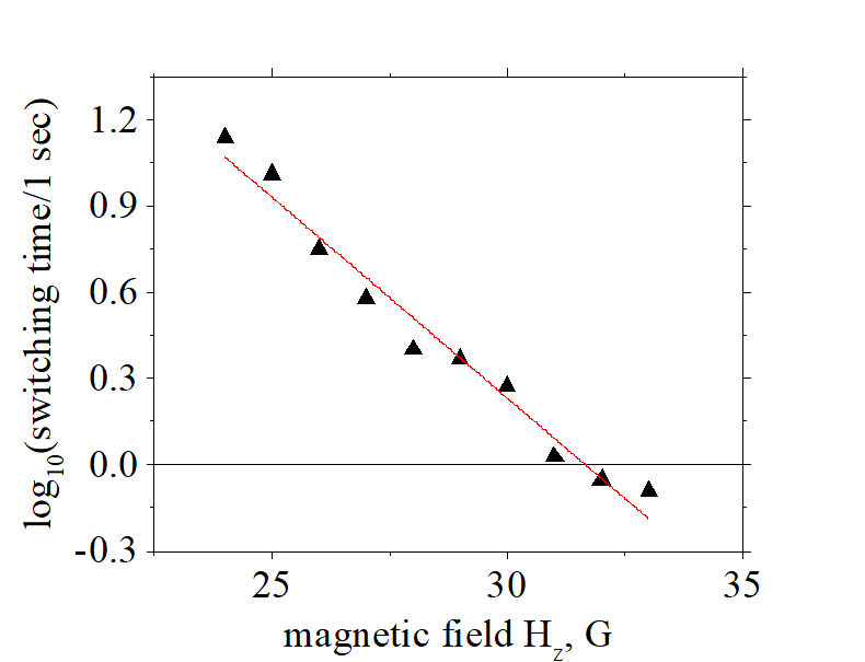
![]() Calculation Example 1 (left graph) Volt54A Ta(2.5 nm):FeB(1.1 nm)
Calculation Example 1 (left graph) Volt54A Ta(2.5 nm):FeB(1.1 nm)
Linear fit: 4.43-0.14·H
coercive field Hc=4.43/0.14=31.6 G
size of nucleation domain=sqrt(51717·0.14/1.4/1.1)=68.5 nm
retention time τret=104.43sec=7.4 hours
parameter Δ =0.5· 0.14·2.5·1000=174
M=1.4 T; Hani=2.5 kG; FeB thickness=1.1 nm;
nanomagnet size: 3 μm x 3 μm
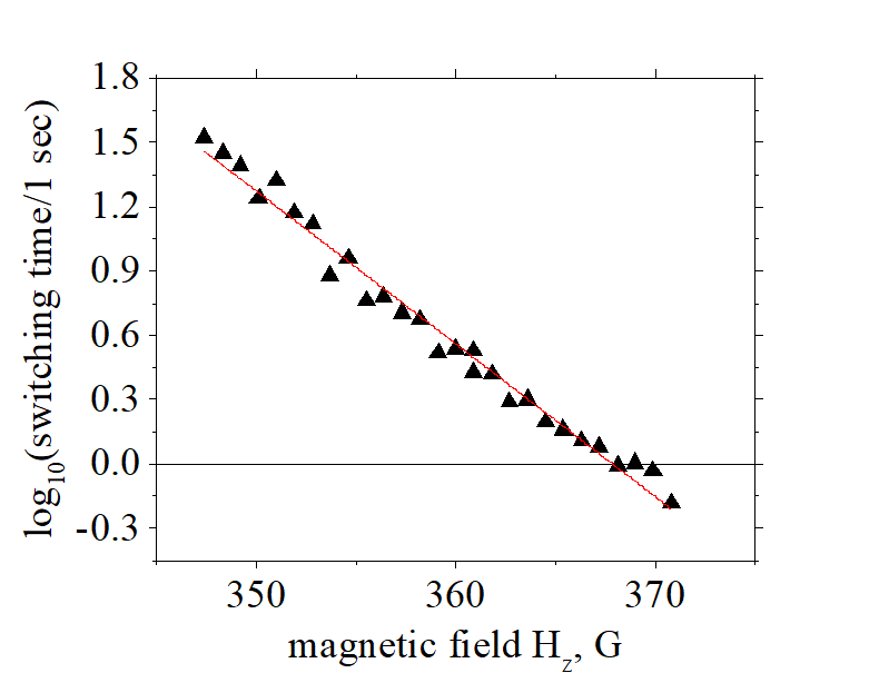
![]() Calculation Example 2 (center graph) Volt59A L68 Ta(8 nm):FeB(0.9 nm) (device:L35)
Calculation Example 2 (center graph) Volt59A L68 Ta(8 nm):FeB(0.9 nm) (device:L35)
Linear fit: 26.224-0.07·H
coercive field Hc=26.224/0.07=367.8 G
size of nucleation domain=sqrt(51717·0.07/1.4/0.9)=54.1 nm
retention time τret=1026.2 sec=3 109 billion years
parameter Δ =0.5· 0.07·7.5·1000=267
M=1.4 T; Hani=7.5 kG; FeB thickness=0.9 nm;
nanomagnet size: 3 μm x 3 μm
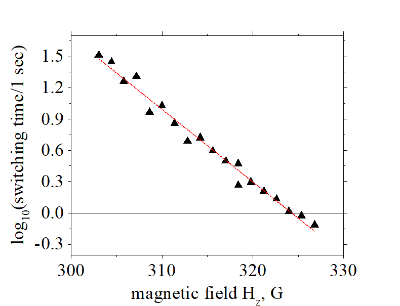
![]() Calculation Example 3 (right graph) Volt40 Ta(2 nm):FeB(1.3 nm) (device:R71)
Calculation Example 3 (right graph) Volt40 Ta(2 nm):FeB(1.3 nm) (device:R71)
Linear fit: 22.5-0.07·H
coercive field Hc=22.5/0.07=324 G
size of nucleation domain=sqrt(51717·0.07/1.4/1.3)=44.4 nm
retention time τret=1022.5sec=1015 years=1,000,000 billion years
parameter Δ =0.5·0.07·4.4·1000=152
M=1.4 T; Hani=4.4 kG; FeB thickness=1.3 nm;
nanomagnet size: 3 μm x 3 μm
Reason 1 ![]() (minor): thickness of FeB
(minor): thickness of FeB![]() FeB of Volt59A is slightly thicker than FeB of Volt54A . As a result, the contribution of the bulk of FeB becomes larger and the film becomes softer.
FeB of Volt59A is slightly thicker than FeB of Volt54A . As a result, the contribution of the bulk of FeB becomes larger and the film becomes softer.
Reason 2 ![]() (major): roughness of FeB interface
(major): roughness of FeB interface ![]() The Ta layer is substantially thicker in Volt59A than in Volt54A . The thicker Ta layer makes smoother the FeB interface and therefore enhances the PMA
The Ta layer is substantially thicker in Volt59A than in Volt54A . The thicker Ta layer makes smoother the FeB interface and therefore enhances the PMA
Reason 1 ;+ Reason 2 leads to the difference in PMA energy between samples. The PMA energy of Volt59A (Hani=7.5 kG) is 1.7 times large than that of Volt40 (Hani=4.4 kG) and 3 times larger that of Volt54A (Hani=2.5 kG)
Reason 3![]() (major): unknown origin
(major): unknown origin ![]() ?????
?????
![]() The huge difference in retention time between Volt54A ( τret=7.4 hours) and Volt40 (τret=1015 years), Volt59A (τret=3 1018 years) cannot be explained by 1.8/3 times difference in the PMA energy.
The huge difference in retention time between Volt54A ( τret=7.4 hours) and Volt40 (τret=1015 years), Volt59A (τret=3 1018 years) cannot be explained by 1.8/3 times difference in the PMA energy.
 Mechanism which makes such a huge difference in τret between Volt54A and Volt40 is still a puzzle
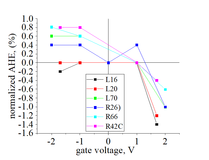
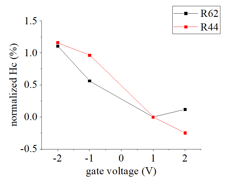
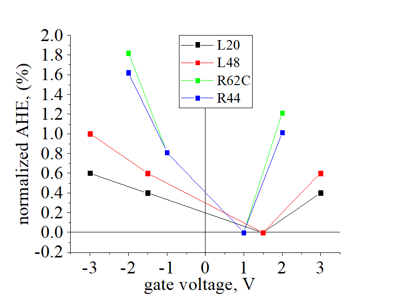
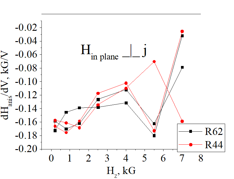
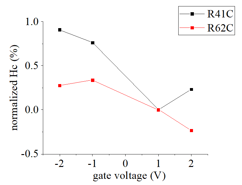
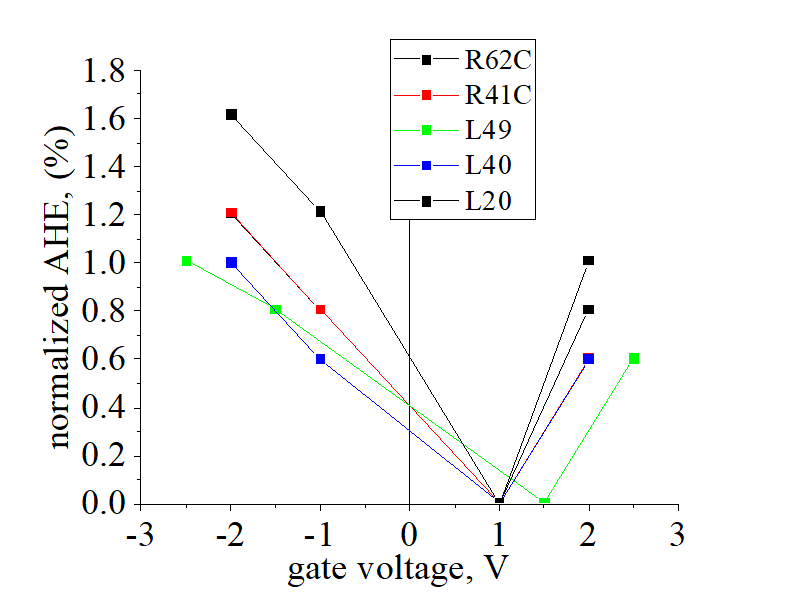
Voltage- Controlled Magnetic Anisotropy (VCMA) effect |
|---|
| Dependence of magnetic properties on gate voltage |
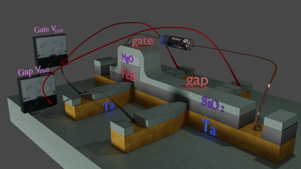
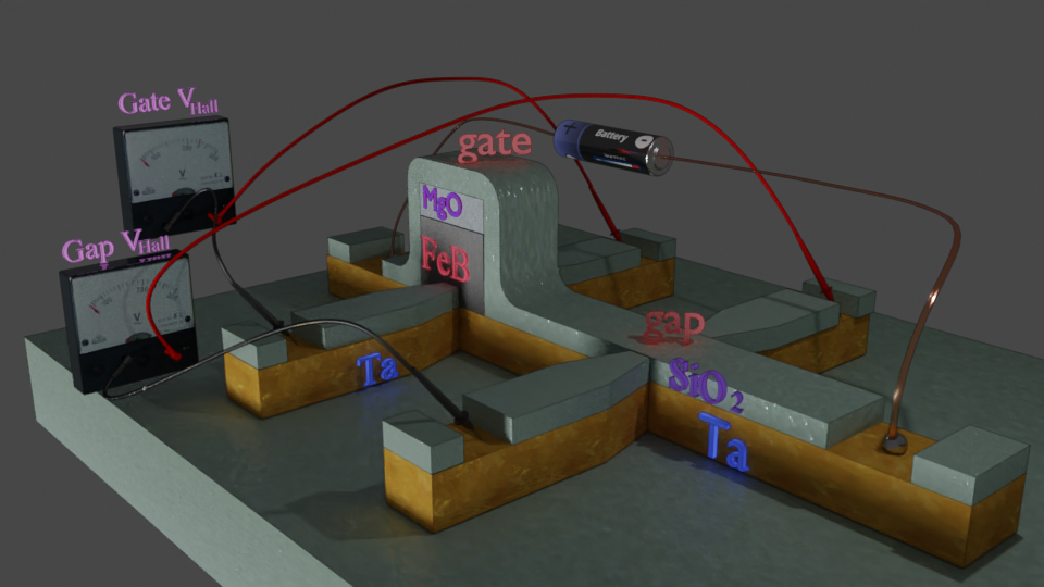
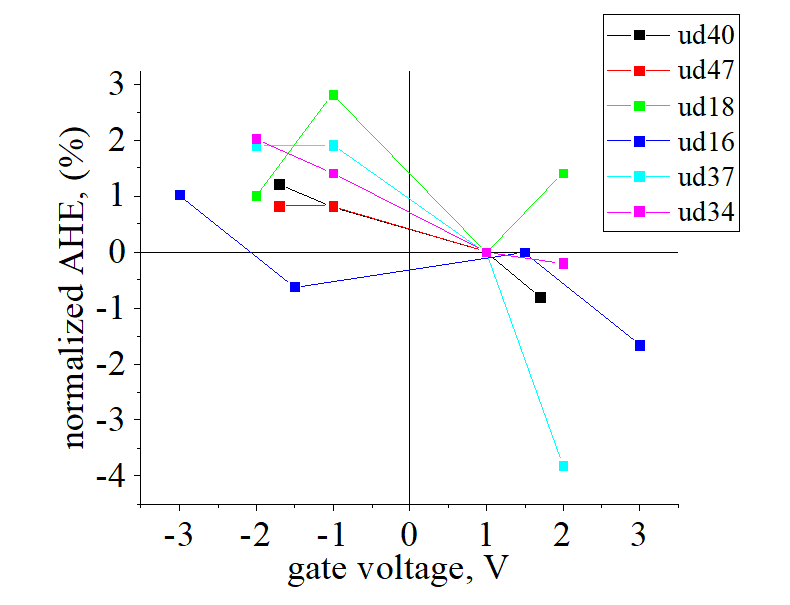
| Magnetic properties of nanomagnet (FeB, shown in grey) are changed when a gate voltage is applied at a metal- isolator interface at the top of the nanomagnet. The source battery provides the bias current through the metallic nanowire and the nanomagnet. The voltmeter measured the Hall voltage, which is created perpendicularly to the bias current. The gate voltage is applied between the top of nanomagnet and the nanowire. Because of thick (~ 10 nm) gate isolator (MgO), the gate voltage does not induce any electrical current. The gate modulation does not change the temperature of the nanomagnet. It is the main merit of the modulation of the magnetic properties of nanomagnet by a gate voltage. The effect, which describes the dependence of the magnetic properties on the gate voltage, is called the Voltage- Controlled Magnetic Anisotropy (VCMA). See details here. |
| |
| click on image to enlarge it |
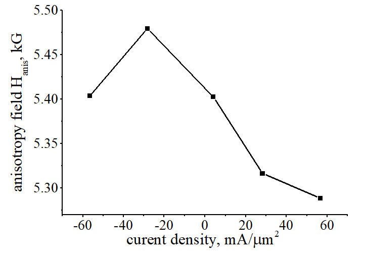
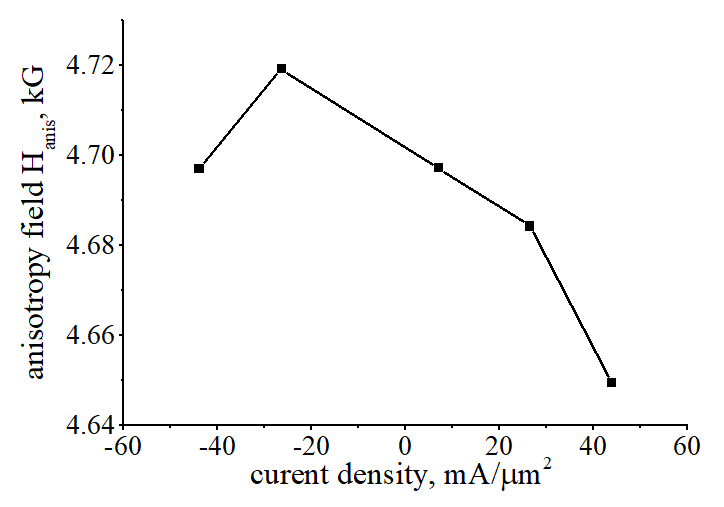
(main idea): ![]() Dependence of magnetic parameters of a nanomagnet on magnitude of current j is measured. Since the gate voltage does not cause any electrical current, there is no influence of heating for this measurement.
Dependence of magnetic parameters of a nanomagnet on magnitude of current j is measured. Since the gate voltage does not cause any electrical current, there is no influence of heating for this measurement.
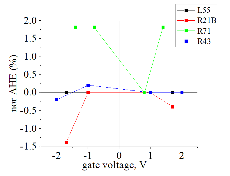
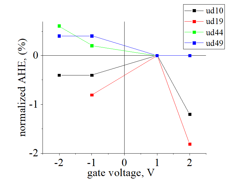
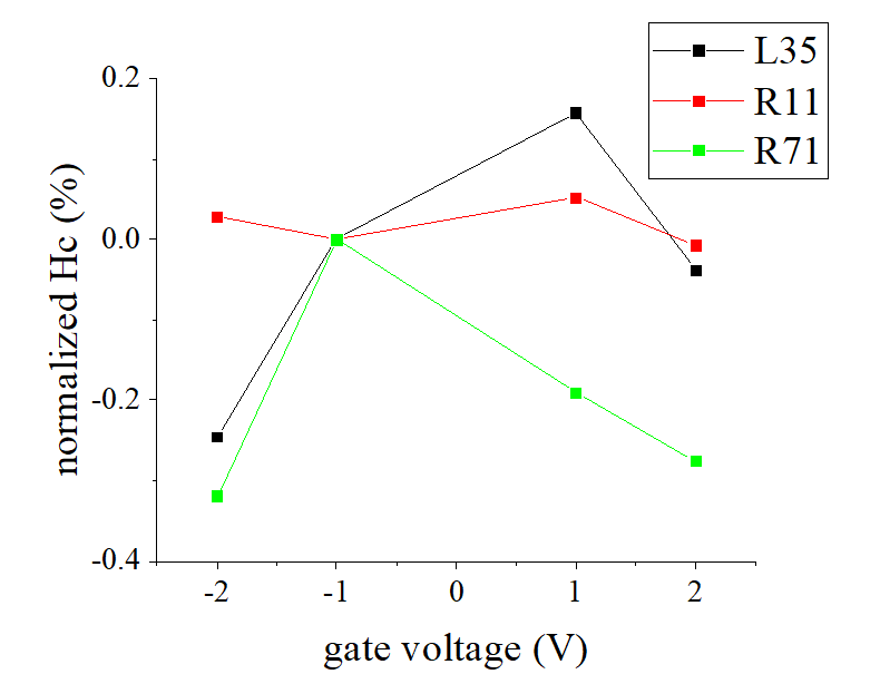
All samples show the same dependence on the gate voltage. All magnetic parameters increased

![]()
(main idea): ![]() Dependence of magnetic parameters of a nanomagnet on magnitude of current j is measured. The heating and therefore the sample temperature is proportional to current square j2.
Dependence of magnetic parameters of a nanomagnet on magnitude of current j is measured. The heating and therefore the sample temperature is proportional to current square j2.
dependence of magnetic parameters on temperature (~j2 ) |
||||||||||||
|---|---|---|---|---|---|---|---|---|---|---|---|---|
|
||||||||||||
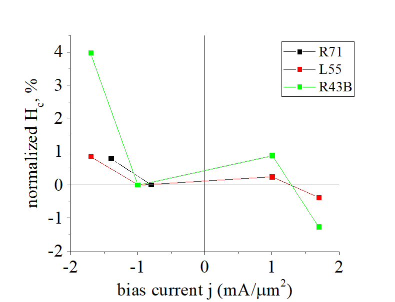
All magnetic parameters depends on current j as A · j2 +B · j, where parameter A describes temperature dependence and parameter B describes dependence on polarity of j (SOT effect) |
||||||||||||
| note: heating and therefore the sample temperature is proportional to j2. | ||||||||||||
| click on image to enlarge it |
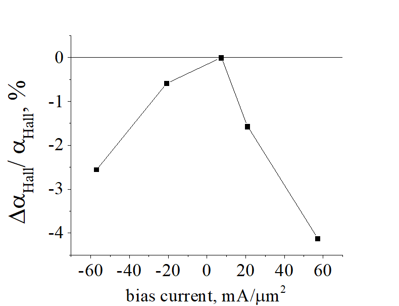
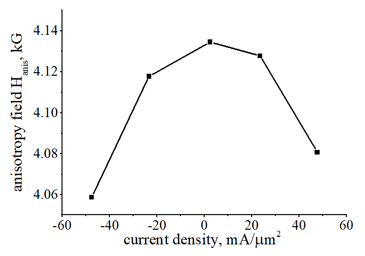
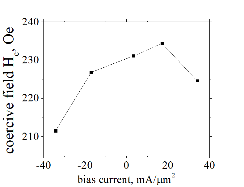
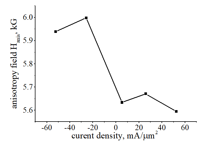
 (SOT effect)
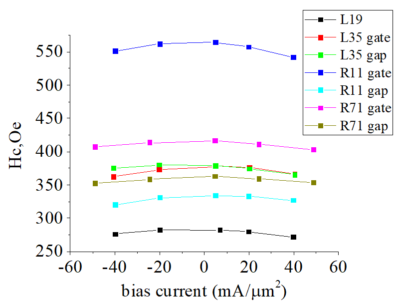
 Spin-orbit torque (SOT) effect |
|---|
| dependence of magnetic properties on polarity of bias current |
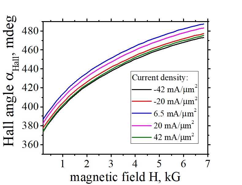
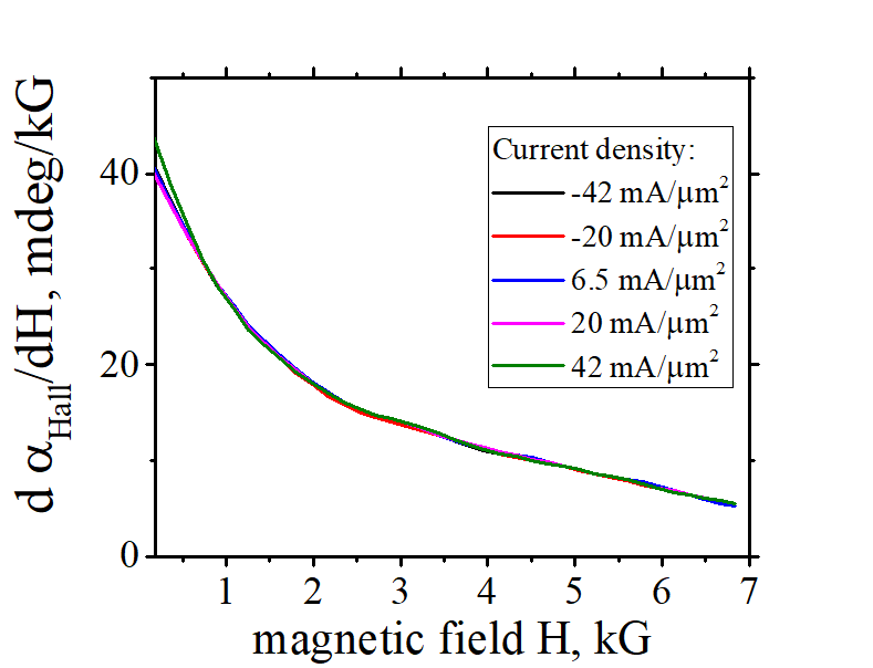
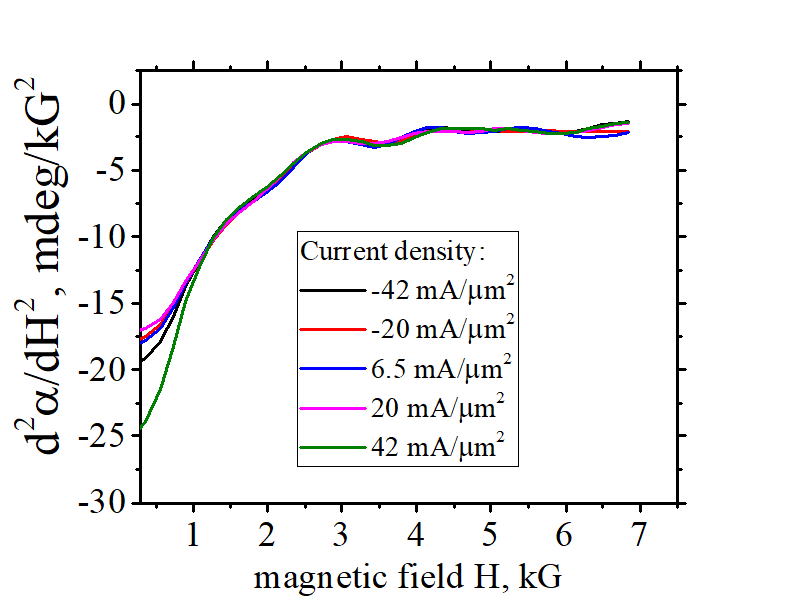
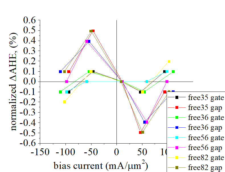
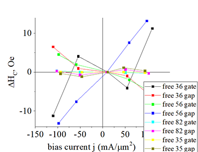
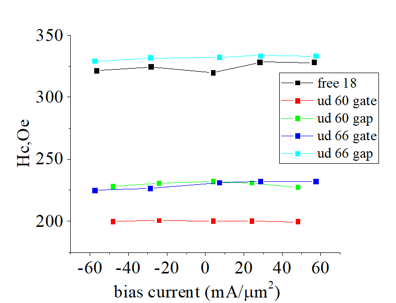
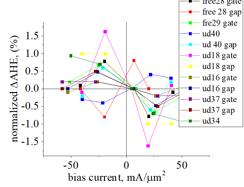
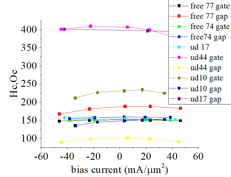
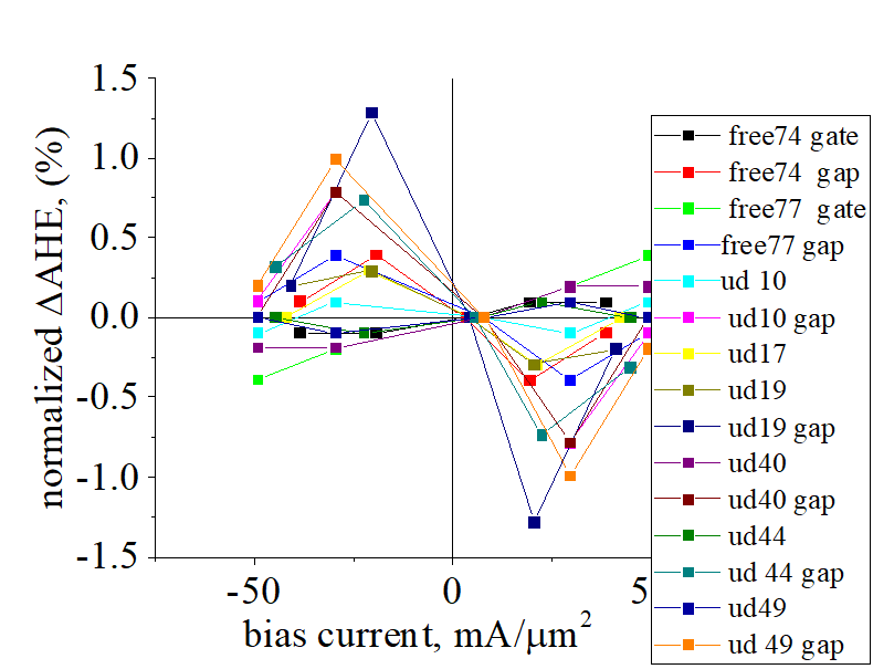
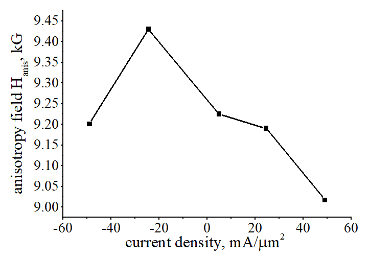
| Magnetic properties of nanomagnet are changed when the value of bias is changed. The source battery provides the bias current through the metallic nanowire and the nanomagnet. The voltmeter measured the Hall voltage, which is created perpendicularly to the bias current. Since the used current density is relatively large ~ 50 mA/um2 (otherwise the Hall voltage is to small to detect), the temperature of the nanomagnet is changed when the magnitude of the current change. Additionally, the magnetic properties of the nanomagnet depend on the polarity of the current. This effect is called Spin- Orbit Torque (SOT). (See details here) |
| |
| click on image to enlarge it |
(main idea): ![]() Dependence of magnetic parameters of a nanomagnet on polarity of current j is measured. In order to avoid the influence of heating due to the current, the same magnetic parameters is measured for two opposite currents. The difference of measured parameters ids due to the SOT effect.
Dependence of magnetic parameters of a nanomagnet on polarity of current j is measured. In order to avoid the influence of heating due to the current, the same magnetic parameters is measured for two opposite currents. The difference of measured parameters ids due to the SOT effect.

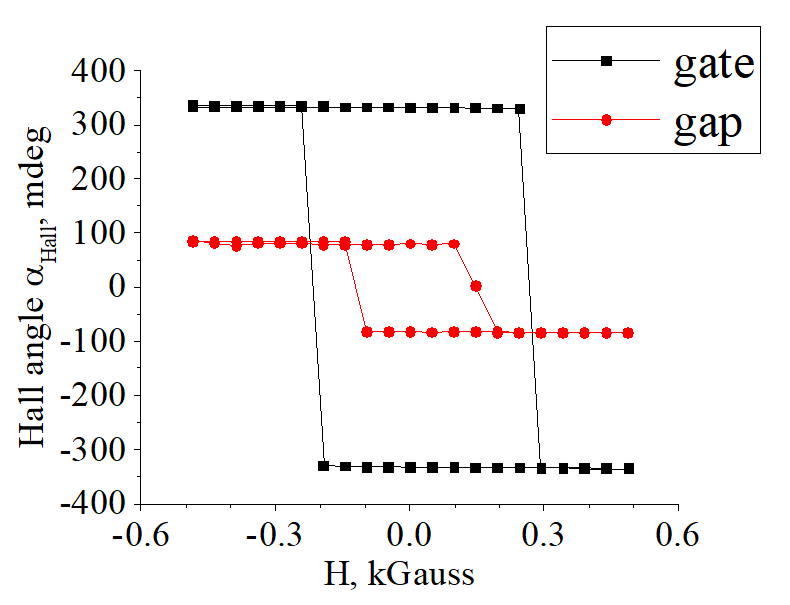
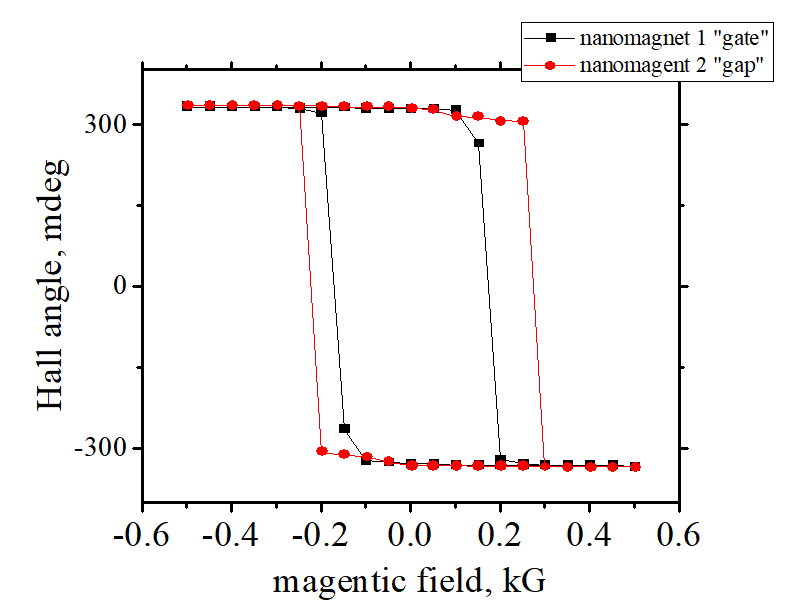
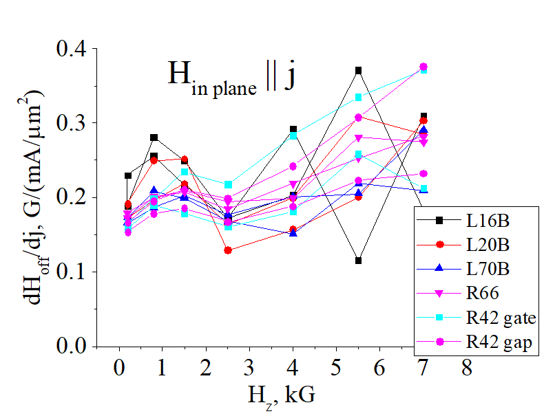
Measurement method: in gate and gap regions |
||||
|
||||
| (note): distance between gate and gap probes is 15 μm in all samples (EB or stepper- made) | ||||
| click on image to enlarge it |
(note) ![]() Thickness of ferromagnetic FeB layer is only 1 nm. It is hard to stop at a precise designed etched thickness.
Thickness of ferromagnetic FeB layer is only 1 nm. It is hard to stop at a precise designed etched thickness.
(note)  Etched materials were monitored during etching. Sensitivity of monitoring of Mg is high. Sensitivity of monitoring of Si,Fe,B,O2 is very low, because of chamber contamination by these elements. Sensitivity of monitoring of Ta is moderate/ low.
(note)![]() It is critically important to monitor that Ta layer is not etched out.
It is critically important to monitor that Ta layer is not etched out.
It is much better to make the contact to FeB layer rather than to Ta layer. However, sometimes it is difficult (but possible) to stop inside FeB layer.
The reason why it is better to stop etching inside FeB is following. After the etching the hole for the contact and before the deposition of top Au contact the sample are exposed to air. As a result, its top surface is slightly oxidized making unwanted tunnel barrier for contact significantly increasing the contact resistance. If this unwanted tunnel barrier is thin and it is broken during measurement (e.g. under 1 V). On FeB the oxide is very thin and it has almost no influence on the contact resistance. The oxide on Ta is strong, hard to break and it has a substantial resistance. The worse case is the oxide on tungsten (W). It is very strong and highly resistant.
In all most- recent samples I can reliably stop etching for the contact inside FeB layer
Etching depth & coercive loop |
||||
Full etch |
||||
|---|---|---|---|---|
|
||||
Half etched |
||||
|
||||
Unetched |
||||
|
||||
two nanomagnet on one naowire |
||||||
|
||||||
| Click on image to enlarge it |
Magneto- static properties |
|||||||||
|
|||||||||
| Click on image to enlarge it |
Conductivity: 0.023-0.029 S/m2
Anisotropy field Hanis =4.2 kGauss
Coercive field = 170 Oe-220 Oe;
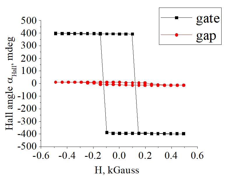
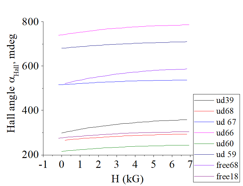
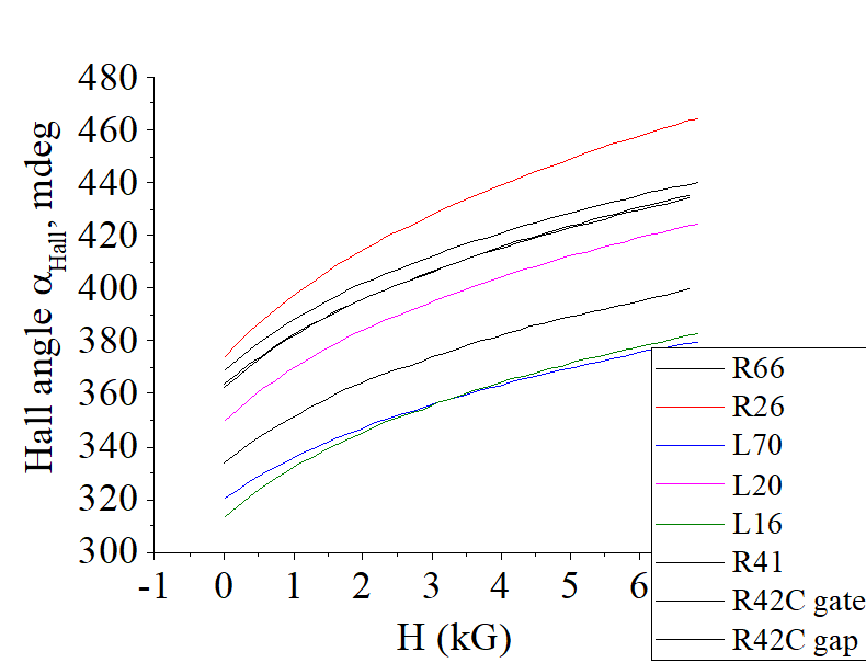
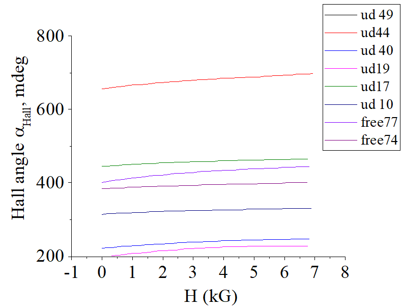
Hall angle measured=290- 390 deg
Intrinsic Hall angle of FeB= 736- 990 mdeg;
Gap region etched: FeB is fully etched, stopped at FeB/ Ta interface
ample:( R21 gate) ![]() αISHE,0.5= 222 mdeg; αAHE,0.5= 753 mdeg; αOHE=0.2 mdeg/kG; Hp=13.6 kG;
αISHE,0.5= 222 mdeg; αAHE,0.5= 753 mdeg; αOHE=0.2 mdeg/kG; Hp=13.6 kG;
range of Hp: 9.7 kG -21.6 mean Hp: 14.78 kG
![]()
![]() magnetization- switching parameters:
magnetization- switching parameters:
retention time τret : 1021 s
size of nucleation domain: 40 nm;
coercive field Hc: 310 Oe
parameter Δ : 120
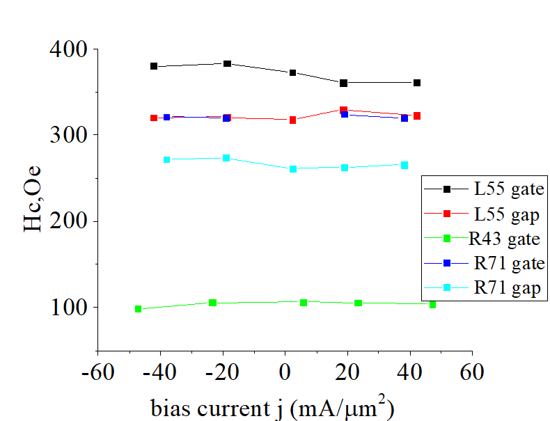
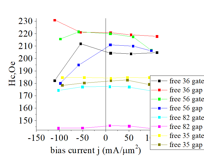
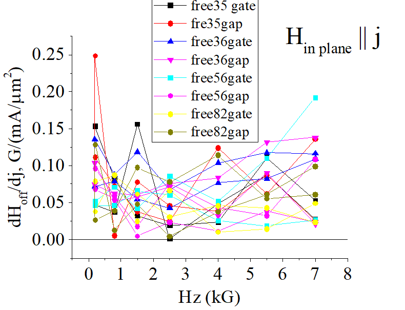
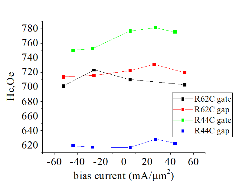
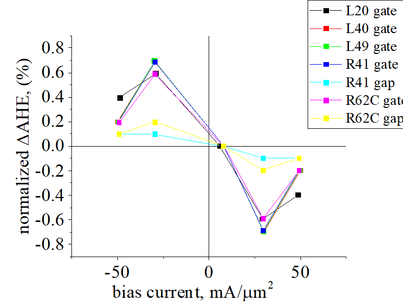
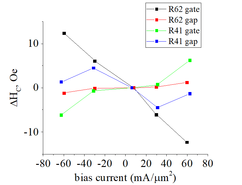
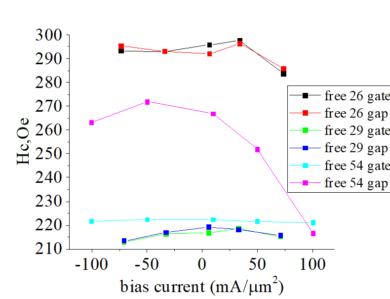
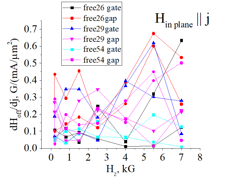
Spin- orbit torque
|
||||||||||||||||||||||||
dependence of magnetic parameters on current and current polarity flowing through a nanomagnet |
||||||||||||||||||||||||
|---|---|---|---|---|---|---|---|---|---|---|---|---|---|---|---|---|---|---|---|---|---|---|---|---|
|
||||||||||||||||||||||||
| Click on image to enlarge it |
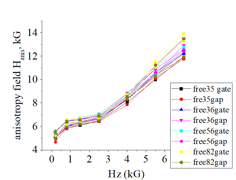
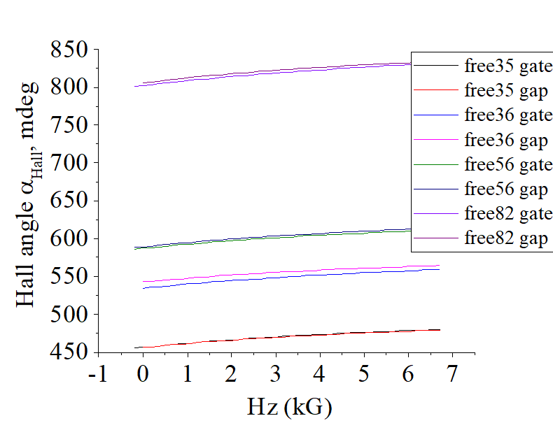
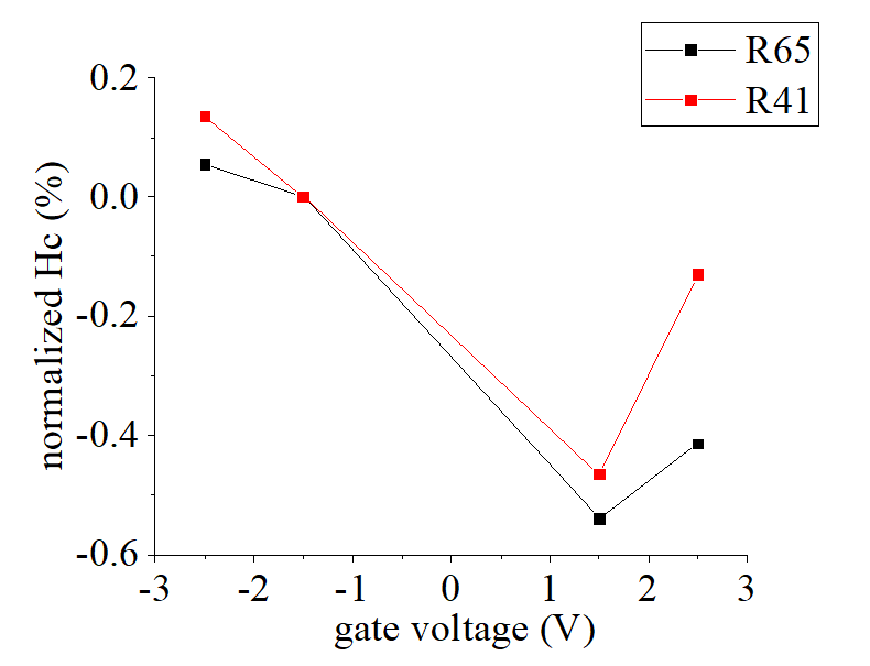
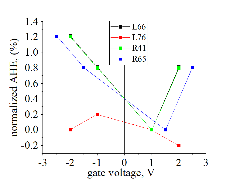
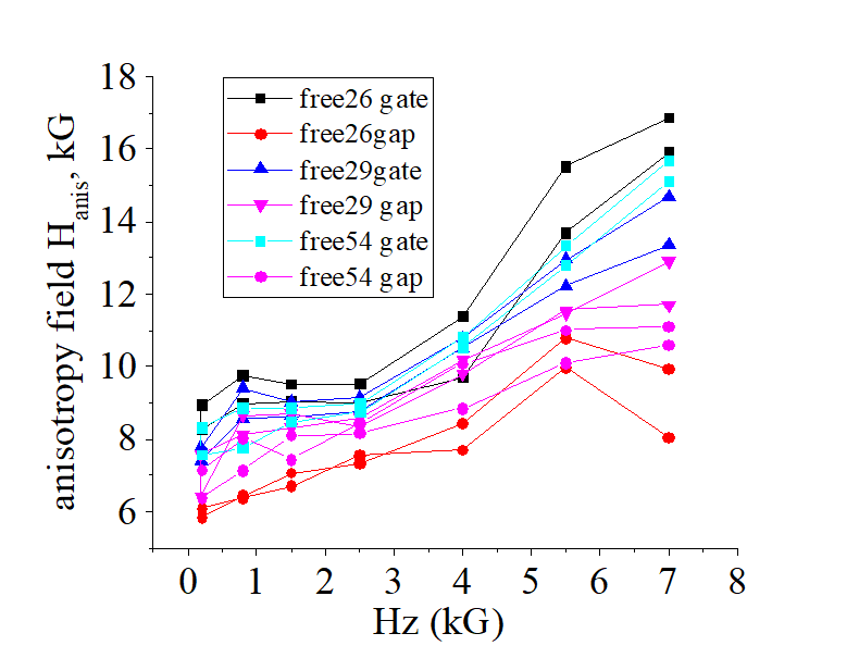
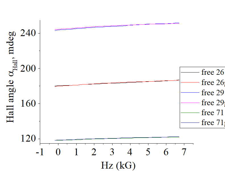
 Voltage controlled magnetic anisotropy (VCMA)
|
||||||||||||||||||||
dependence of magnetic parameters on a gate voltage |
||||||||||||||||||||
|---|---|---|---|---|---|---|---|---|---|---|---|---|---|---|---|---|---|---|---|---|
|
||||||||||||||||||||
| Click on image to enlarge it |
Magneto- static properties |
|||||||||
|
|||||||||
| Click on image to enlarge it |
Conductivity: 0.039-0.62 S/m2
Anisotropy field Hanis =5kGauss
Coercive field = 170 Oe-220 Oe;
Hall angle measured=450- 800 deg
Intrinsic Hall angle of FeB= ;
Gap region etched: stopped at MgO/ FeB interface
sample:( free36 gate) ![]() αISHE,0.5= 213 mdeg; αAHE,0.5= 1777 mdeg; αOHE=0.2 mdeg/kG; Hp=9.72 kG;
αISHE,0.5= 213 mdeg; αAHE,0.5= 1777 mdeg; αOHE=0.2 mdeg/kG; Hp=9.72 kG;
![]()
![]() magnetization- switching parameters:
magnetization- switching parameters:
retention time τret : 1014 s
size of nucleation domain: 45 nm;
coercive field Hc: 200 Oe
parameter Δ : 150
Spin- orbit torque
|
||||||||||||||||||||||||
dependence of magnetic parameters on current and current polarity flowing through a nanomagnet |
||||||||||||||||||||||||
|---|---|---|---|---|---|---|---|---|---|---|---|---|---|---|---|---|---|---|---|---|---|---|---|---|
|
||||||||||||||||||||||||
| Click on image to enlarge it |
Magneto- static properties |
|||||||||
|
|||||||||
| Click on image to enlarge it |
Conductivity: 0.04-0.06 S/m2
Anisotropy field Hanis =2.2 kGauss-6 kGauss
Coercive field = 200 Oe-330 Oe;
Hall angle measured αHall, measured =290- 750 mdeg
Intrinsic Hall angle of FeB αHall, FeB= 1015 - 2625 mdeg;
Gap region etched: FeB is partially etched, stopped in middle of FeCoB
sample:( ud66) ![]() αISHE,0.5= 274 mdeg; αAHE,0.5=2324 mdeg; αOHE=0.2 mdeg/kG; Hp=5.84 kG;
αISHE,0.5= 274 mdeg; αAHE,0.5=2324 mdeg; αOHE=0.2 mdeg/kG; Hp=5.84 kG;
Spin- orbit torque
|
||||||||||||||||||||||||
dependence of magnetic parameters on current and current polarity flowing through a nanomagnet |
||||||||||||||||||||||||
|---|---|---|---|---|---|---|---|---|---|---|---|---|---|---|---|---|---|---|---|---|---|---|---|---|
|
||||||||||||||||||||||||
| Click on image to enlarge it |
Voltage controlled magnetic anisotropy (VCMA)
|
||||||||||||||||||||
dependence of magnetic parameters on a gate voltage |
||||||||||||||||||||
|---|---|---|---|---|---|---|---|---|---|---|---|---|---|---|---|---|---|---|---|---|
|
||||||||||||||||||||
| Click on image to enlarge it |
Magneto- static properties |
|||||||||
|
|||||||||
| Click on image to enlarge it |
Conductivity: 0.055-0.06 S/m2
Anisotropy field Hanis =2.5 kGauss
Coercive field = 20 Oe-70 Oe;
Hall angle measured αHall, measured =320- 370 mdeg
Intrinsic Hall angle of FeB αHall, FeB= 1047 - 1211 mdeg;
Gap region etched: FeB is partially etched, stopped in middle of FeB
sample:( L70) ![]() αISHE,0.5= 351 mdeg; αAHE,0.5= 695 mdeg; αOHE=0.2 mdeg/kG; Hp=5.84 kG;
αISHE,0.5= 351 mdeg; αAHE,0.5= 695 mdeg; αOHE=0.2 mdeg/kG; Hp=5.84 kG;
Spin- orbit torque
|
||||||||||||||||||||||||
dependence of magnetic parameters on current and current polarity flowing through a nanomagnet |
||||||||||||||||||||||||
|---|---|---|---|---|---|---|---|---|---|---|---|---|---|---|---|---|---|---|---|---|---|---|---|---|
|
||||||||||||||||||||||||
| Click on image to enlarge it |
Voltage controlled magnetic anisotropy (VCMA)
|
||||||||||||||||||||
dependence of magnetic parameters on a gate voltage |
||||||||||||||||||||
|---|---|---|---|---|---|---|---|---|---|---|---|---|---|---|---|---|---|---|---|---|
|
||||||||||||||||||||
| Click on image to enlarge it |
Magneto- static properties |
|||||||||
|
|||||||||
| Click on image to enlarge it |
Conductivity: 0.037-0.06 S/m2
Anisotropy field Hanis =2 kGauss
Coercive field = 5 Oe-50 Oe;
Hall angle measured αHall, measured =350-400 mdeg
Intrinsic Hall angle of FeB αHall, FeB= 1145 - 1309 mdeg;
Gap region etched: FeB is partially etched, stopped in middle of FeB
sample:( free28 gate) ![]() αISHE,0.5= 551 mdeg; αAHE,0.5= 675 mdeg; αOHE=0.2 mdeg/kG; Hp=3.954 kG;
αISHE,0.5= 551 mdeg; αAHE,0.5= 675 mdeg; αOHE=0.2 mdeg/kG; Hp=3.954 kG;
Spin- orbit torque
|
||||||||||||||||||||||||
dependence of magnetic parameters on current and current polarity flowing through a nanomagnet |
||||||||||||||||||||||||
|---|---|---|---|---|---|---|---|---|---|---|---|---|---|---|---|---|---|---|---|---|---|---|---|---|
|
||||||||||||||||||||||||
| Click on image to enlarge it |
Voltage controlled magnetic anisotropy (VCMA)
|
||||||||||||||||||||
dependence of magnetic parameters on a gate voltage |
||||||||||||||||||||
|---|---|---|---|---|---|---|---|---|---|---|---|---|---|---|---|---|---|---|---|---|
|
||||||||||||||||||||
| Click on image to enlarge it |
Magneto- static properties |
|||||||||
|
|||||||||
| Click on image to enlarge it |
Conductivity: 0.028-0.038 S/m2
Anisotropy field Hanis =4 kGauss-11 kGauss
Coercive field = 150 Oe-225 Oe; (a few: 400 Oe,90 Oe)
Hall angle measured αHall, measured =200- 650 mdeg
Intrinsic Hall angle of FeB αHall, FeB= 1311 - 4261 mdeg;;
Gap region etched: FeB is fully (partiality) etched, stopped at Ta/FeB interface (in middle of FeCoB)
sample:(ud40) ![]() αISHE,0.5= 323.8 mdeg; αAHE,0.5= 1141 mdeg; αOHE=0.2 mdeg/kG; Hp=7.25 kG;
αISHE,0.5= 323.8 mdeg; αAHE,0.5= 1141 mdeg; αOHE=0.2 mdeg/kG; Hp=7.25 kG;
Spin- orbit torque
|
||||||||||||||||||||||||
dependence of magnetic parameters on current and current polarity flowing through a nanomagnet |
||||||||||||||||||||||||
|---|---|---|---|---|---|---|---|---|---|---|---|---|---|---|---|---|---|---|---|---|---|---|---|---|
|
||||||||||||||||||||||||
| Click on image to enlarge it |
Voltage controlled magnetic anisotropy (VCMA)
|
||||||||||||||||||||
dependence of magnetic parameters on a gate voltage |
||||||||||||||||||||
|---|---|---|---|---|---|---|---|---|---|---|---|---|---|---|---|---|---|---|---|---|
|
||||||||||||||||||||
| Click on image to enlarge it |
Magneto- static properties |
|||||||||
|
|||||||||
| Click on image to enlarge it |
Conductivity: 0.044-0.055 S/m2
Anisotropy field Hanis =4.8 kGauss
Coercive field = 200 Oe-330 Oe;
Hall angle measured αHall, measured =175- 235 mdeg
Intrinsic Hall angle of FeB αHall, FeB= 970- 1303 mdeg;
Gap region etched: FeB is fully etched, stopped at Ta/FeCoB interface
sample:( L66) ![]() αISHE,0.5= 241 mdeg; αAHE,0.5= 930 mdeg; αOHE=0.2 mdeg/kG; Hp=5.5 kG;
αISHE,0.5= 241 mdeg; αAHE,0.5= 930 mdeg; αOHE=0.2 mdeg/kG; Hp=5.5 kG;
Spin- orbit torque
|
||||||||||||||||||||||||
dependence of magnetic parameters on current and current polarity flowing through a nanomagnet |
||||||||||||||||||||||||
|---|---|---|---|---|---|---|---|---|---|---|---|---|---|---|---|---|---|---|---|---|---|---|---|---|
|
||||||||||||||||||||||||
| Click on image to enlarge it |
Voltage controlled magnetic anisotropy (VCMA)
|
||||||||||||||||||||
dependence of magnetic parameters on a gate voltage |
||||||||||||||||||||
|---|---|---|---|---|---|---|---|---|---|---|---|---|---|---|---|---|---|---|---|---|
|
||||||||||||||||||||
| Click on image to enlarge it |
Magneto- static properties |
|||||||||
|
|||||||||
| Click on image to enlarge it |
Conductivity: 0.02-0.027 S/m2
Anisotropy field Hanis =5 kGauss
Coercive field = 620 Oe-740 Oe;
Hall angle measured αHall, measured =110- 150 deg
Intrinsic Hall angle of FeB αHall, FeB= 610- 831 mdeg;;
Gap region etched: FeB is partially etched, stopped in middle of FeCoB
sample:( L20) ![]() αISHE,0.5= 65 mdeg; αAHE,0.5= 594 mdeg; αOHE=0.2 mdeg/kG; Hp=8.9 kG;
αISHE,0.5= 65 mdeg; αAHE,0.5= 594 mdeg; αOHE=0.2 mdeg/kG; Hp=8.9 kG;
Spin- orbit torque
|
||||||||||||||||||||||||
dependence of magnetic parameters on current and current polarity flowing through a nanomagnet |
||||||||||||||||||||||||
|---|---|---|---|---|---|---|---|---|---|---|---|---|---|---|---|---|---|---|---|---|---|---|---|---|
|
||||||||||||||||||||||||
| Click on image to enlarge it |
Voltage controlled magnetic anisotropy (VCMA)
|
||||||||||||||||||||
dependence of magnetic parameters on a gate voltage |
||||||||||||||||||||
|---|---|---|---|---|---|---|---|---|---|---|---|---|---|---|---|---|---|---|---|---|
|
||||||||||||||||||||
| Click on image to enlarge it |
Magneto- static properties |
|||||||||
|
|||||||||
| Click on image to enlarge it |
Conductivity: 0.048-0.051 S/m2
Anisotropy field Hanis =6.5 kGauss-8.5 kGauss
Coercive field = 200 Oe-330 Oe;
Hall angle measured αHall, measured =360- 470 mdeg
Intrinsic Hall angle of FeB αHall, FeB=2160- 2820 mdeg;
Gap region etched: FeCoB is partially etched, stopped in middle of FeCoB
sample:( R41 gate) ![]() αISHE,0.5= 377 mdeg; αAHE,0.5= 1497 mdeg; αOHE=0.2 mdeg/kG; Hp=8.8 kG;
αISHE,0.5= 377 mdeg; αAHE,0.5= 1497 mdeg; αOHE=0.2 mdeg/kG; Hp=8.8 kG;
Spin- orbit torque
|
||||||||||||||||||||||||
dependence of magnetic parameters on current and current polarity flowing through a nanomagnet |
||||||||||||||||||||||||
|---|---|---|---|---|---|---|---|---|---|---|---|---|---|---|---|---|---|---|---|---|---|---|---|---|
|
||||||||||||||||||||||||
| Click on image to enlarge it |
Voltage controlled magnetic anisotropy (VCMA)
|
||||||||||||||||||||
dependence of magnetic parameters on a gate voltage |
||||||||||||||||||||
|---|---|---|---|---|---|---|---|---|---|---|---|---|---|---|---|---|---|---|---|---|
|
||||||||||||||||||||
| Click on image to enlarge it |
Magneto- static properties |
|||||||||
|
|||||||||
| Click on image to enlarge it |
Conductivity: 0.048-0.052 S/m2
Anisotropy field Hanis =8 kGauss-11 kGauss
Coercive field = 280 Oe-550 Oe;
Hall angle measured αHall, measured =125- 145 mdeg
Intrinsic Hall angle of FeB αHall, FeB= 1236 -1434 mdeg;
Gap region etched: FeB is partially etched, stopped in middle of FeCoB
Spin- orbit torque
|
||||||||||||||||||||||||
dependence of magnetic parameters on current and current polarity flowing through a nanomagnet |
||||||||||||||||||||||||
|---|---|---|---|---|---|---|---|---|---|---|---|---|---|---|---|---|---|---|---|---|---|---|---|---|
|
||||||||||||||||||||||||
| Click on image to enlarge it |
Voltage controlled magnetic anisotropy (VCMA)
|
||||||||||||||||||||
dependence of magnetic parameters on a gate voltage |
||||||||||||||||||||
|---|---|---|---|---|---|---|---|---|---|---|---|---|---|---|---|---|---|---|---|---|
|
||||||||||||||||||||
| Click on image to enlarge it |
Magneto- static properties |
|||||||||
|
|||||||||
| Click on image to enlarge it |
Conductivity: 0.02-0.054 S/m2
Anisotropy field Hanis =6 kGauss-9 kGauss
Coercive field = 220 Oe-290 Oe;
Hall angle measured αHall, measured =120- 240 mdeg
Intrinsic Hall angle of FeB αHall, FeB= 1186- 2373 mdeg;;
Gap region etched: FeB is not etched, stopped at MgO/FeB interface
sample:( free71gate) ![]() αISHE,0.5= 141.25 mdeg; αAHE,0.5= 1636.1 mdeg; αOHE=0.2 mdeg/kG; Hp=10.46 kG;
αISHE,0.5= 141.25 mdeg; αAHE,0.5= 1636.1 mdeg; αOHE=0.2 mdeg/kG; Hp=10.46 kG;
Spin- orbit torque
|
||||||||||||||||||||||||
dependence of magnetic parameters on current and current polarity flowing through a nanomagnet |
||||||||||||||||||||||||
|---|---|---|---|---|---|---|---|---|---|---|---|---|---|---|---|---|---|---|---|---|---|---|---|---|
|
||||||||||||||||||||||||
| Click on image to enlarge it |
Voltage controlled magnetic anisotropy (VCMA)
no data
![]()
![]() I am strongly against a fake and "highlight" research
I am strongly against a fake and "highlight" research ![]()
![]()
![]()
![]()
![]()
![]()
I will try to answer your questions as soon as possible