Dr. Vadym Zayets
v.zayets(at)gmail.com
My Research and Inventions
click here to see all content |

Dr. Vadym Zayetsv.zayets(at)gmail.com |
|
|
more Chapters on this topic:IntroductionTransport Eqs.Spin Proximity/ Spin InjectionSpin DetectionBoltzmann Eqs.Band currentScattering currentMean-free pathCurrent near InterfaceOrdinary Hall effectAnomalous Hall effect, AMR effectSpin-Orbit interactionSpin Hall effectNon-local Spin DetectionLandau -Lifshitz equationExchange interactionsp-d exchange interactionCoercive fieldPerpendicular magnetic anisotropy (PMA)Voltage- controlled magnetism (VCMA effect)All-metal transistorSpin-orbit torque (SO torque)What is a hole?spin polarizationCharge accumulationMgO-based MTJMagneto-opticsSpin vs Orbital momentWhat is the Spin?model comparisonQuestions & AnswersEB nanotechnologyReticle 11
more Chapters on this topic:IntroductionTransport Eqs.Spin Proximity/ Spin InjectionSpin DetectionBoltzmann Eqs.Band currentScattering currentMean-free pathCurrent near InterfaceOrdinary Hall effectAnomalous Hall effect, AMR effectSpin-Orbit interactionSpin Hall effectNon-local Spin DetectionLandau -Lifshitz equationExchange interactionsp-d exchange interactionCoercive fieldPerpendicular magnetic anisotropy (PMA)Voltage- controlled magnetism (VCMA effect)All-metal transistorSpin-orbit torque (SO torque)What is a hole?spin polarizationCharge accumulationMgO-based MTJMagneto-opticsSpin vs Orbital momentWhat is the Spin?model comparisonQuestions & AnswersEB nanotechnologyReticle 11
|
Volt 53B Ta(2.5 nm)/FeBCo(x=0.3, 1 nm) / MgO(7 nm)/ Ta(1nm)/ Ru(5 nm))Measurement of magnetic and magneto- transport properties of nanomagnets. Measurement data.Abstract:High- precision, high- reproducibility, high- repeatability measurement of magnetic and magneto- transport properties of ferromagnetic nanomagnets using the Hall effectHigh-precision measurement of effect of spin-orbit torque (SOT effect): Dependence of magnetic and magneto- transport properties on electrical currentHigh-precision measurement of effect of voltage-controlled magnetic anisotropy (VCMA effect): Dependence of magnetic and magneto- transport properties on a gate voltage
|
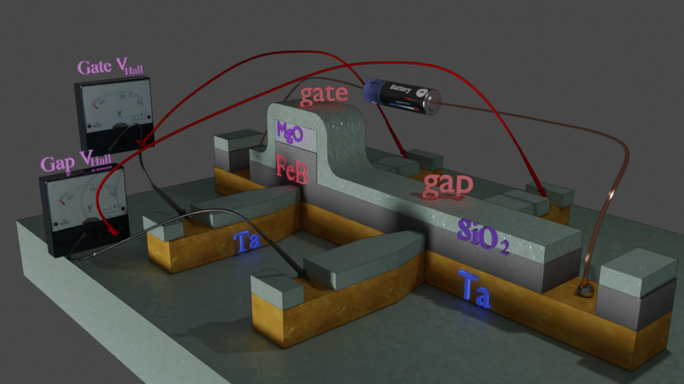
Nanowire with two Hall probes |
 |
Measured hysteresis loop (See below) for gap regions indicates that the etching was stopped in middle of FeCoB layer |
| click on image to enlarge it |
(1.2) Spin-orbit torque: Measurement of dependence of Hall angle, Anomalous Hall effect (AHE), Inverse Spin Hall effect on current magnitude and polarity.
(1.3) VCMA: Measurement of dependence of Hall angle, Anomalous Hall effect (AHE), Inverse Spin Hall effect on gate voltage
(measurement 2) ![]() Measurement of anisotropy field vs external perpendicular magnetic field
Measurement of anisotropy field vs external perpendicular magnetic field ![]()
(2.1) Measurement of PMA & Anisotropy field
(2.2) Spin-orbit torque: ""Field- like torque" ""Damp- like torque". Measurement of dependence of PMA on the electrical current .
(2.3) VCMA: ""Field- like torque" ""Damp- like torque". Measurement of dependence of PMA on gate voltage.
(measurement 3) ![]() Measurement of magnetization switching under external perpendicular magnetic field
Measurement of magnetization switching under external perpendicular magnetic field ![]()
(3.1) Measurement of coercive field HC, retention time, size of nucleation domain, parameter delta Δ
(3.2) Spin-orbit torque: Current dependence of magnetization switching parameters.
(3.3) VCMA: dependence of magnetization switching parameters on gate voltage.
(measurement 4) ![]() Measurement of magnetization switching under in-plane bias magnetic field
Measurement of magnetization switching under in-plane bias magnetic field ![]()
(4.1) Measurement of coercive field HC, retention time, size of nucleation domain, parameter delta Δ
(4.2) Spin-orbit torque: Current dependence of magnetization switching parameters.
(4.3) VCMA: dependence of magnetization switching parameters on gate voltage.
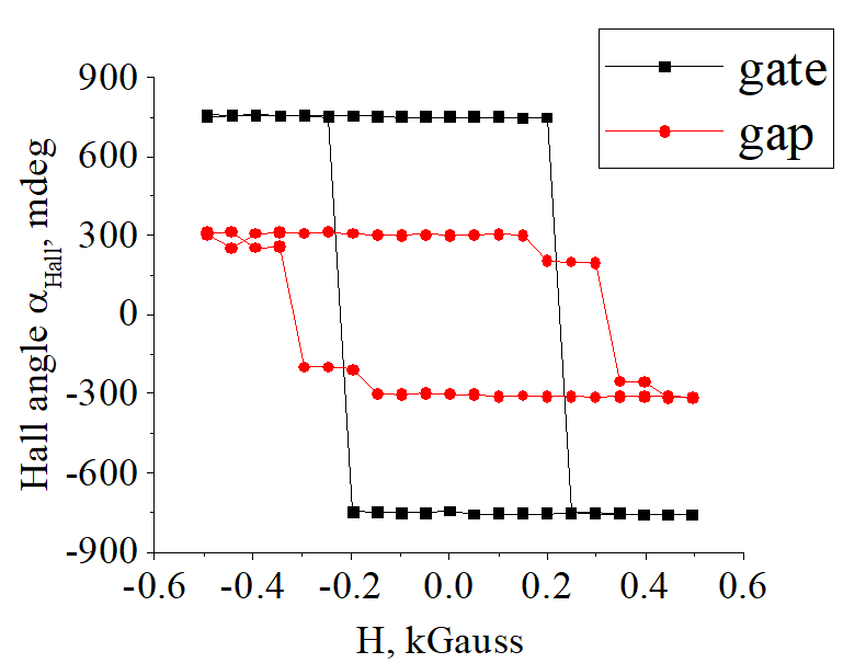
Hysteresis loop |
||||
|
||||
Sample Volt53: Ta(2.5 nm)/ FeBCo(x=0.3, 1 nm) MgO(5.1 nm)/ Ta(1nm)/ Ru(5 nm) |
||||
| click on image to enlarge it |
fabrication: EB only, 18/01/30 day3
MgO 220C/360C
Raw data Volt53.zip (.dat files and origin 9 files)
Conductivity: 0.04-0.06 S/m2
Anisotropy field Hanis =2.2 kGauss-6 kGauss
Coercive field = 200 Oe-330 Oe;
Hall angle measured=290- 750 mdeg
Intrinsic Hall angle of FeB= 1015 - 2625 mdeg;
Gap region etched: FeB is partially etched, stopped in middle of FeCoB
![]()
![]() magnetization- switching parameters:
magnetization- switching parameters: ![]()
![]()
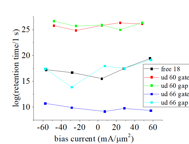
retention time τret
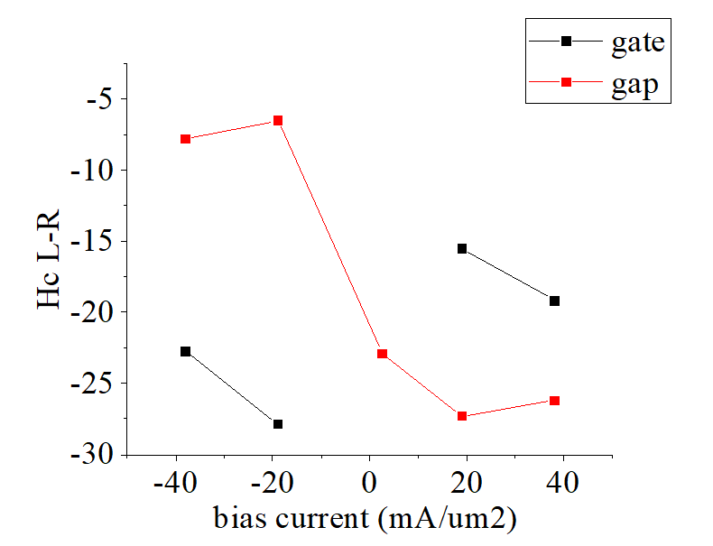
(gate): free18-> 1017 s; ud60-> 1026 s; ud66-> 1010 s; ud67-> 108 s;
(gap): ud60-> 1026 s; ud66-> 1017 s;
Kerr Rotation angle MOKE |
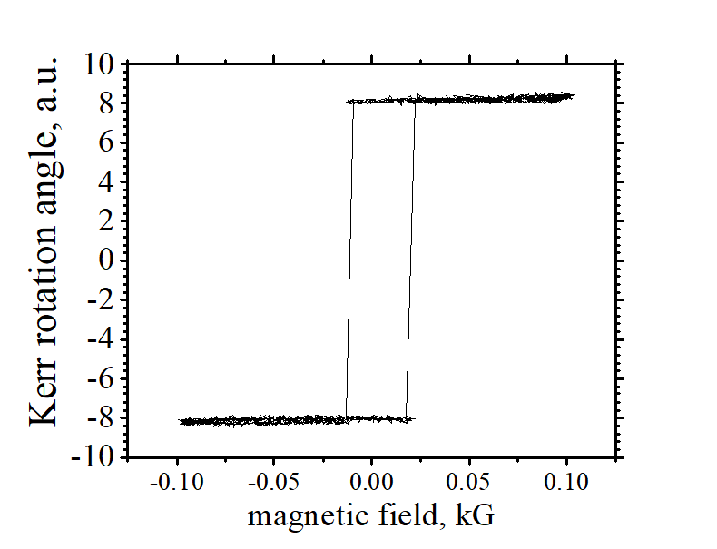 |
data of a plain film before nanofabrication |
| (note) Coercive field and shape of coercive loop is very different for a nanomagnet and film, from which it was fabricated, because of different magnetization switching mechanisms (See here) |
| click on image to enlarge it |
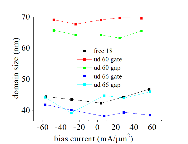
size of nucleation domain:
(gate): free18-> 42 nm; ud60-> 69 nm; ud66-> 35 nm; ud67-> 33 nm;
(gap): ud60-> 64 nm; ud66-> 43 nm;
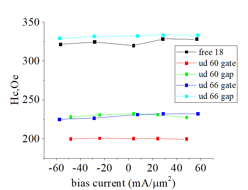
coercive field Hc:
(gate): free18-> 325 Oe; ud60-> 200 Oe; ud66-> 230 Oe; ud67-> 260 Oe;
(gap): ud60-> 230 Oe; ud66-> 330 Oe;
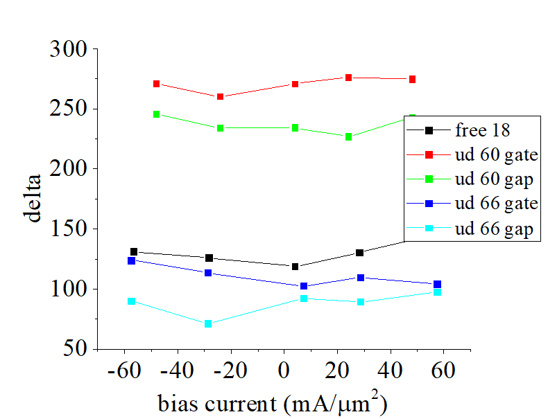
parameter Δ :
(gate): free18-> 130; ud60-> 270; ud66-> 100; ud67->60;
(gap): ud60-> 240; ud66-> 90;
(ud 59): wire width: 400 nm; nanomagnet length: 10 μm; σ = 0.0446 S/m2
(ud 60): wire width: 1000 nm; nanomagnet length: 200 nm; σ = ? S/m2
(ud 66): wire width: 200 nm; nanomagnet length: 500 nm; σ = ? S/m2
(ud 67): wire width: 400 nm; nanomagnet length: 500 nm; σ = 0.0486 S/m2
(ud 68): wire width: 1000 nm; nanomagnet length: 500 nm; σ = 0.040 S/m2
(ud 73): wire width: 400 nm; nanomagnet length: 2000 nm; σ = 0.050 S/m2
(ud 39): wire width: 400 nm; nanomagnet length: 200 nm; σ = 0.0475 S/m2
(free 18): wire width: 1000 nm; nanomagnet length: 200 nm; σ = 0.04 S/m2
(free 68): wire width: 200 nm; lattice: stripe: 300 nm; gap 300 nm: ; σ = 0.064 S/m2
Since the nanowire is double- layer, which consists of Ta and FeCoB layer, the Hall angle αHall, FeB in FeCoB can be calculated from measured Hall angle αHall, measured (See here) as

where 
tFeB, tTa, σFeB,σTa are thicknesses and conductivities of FeCoB and Ta metals.
kdouble=3.5
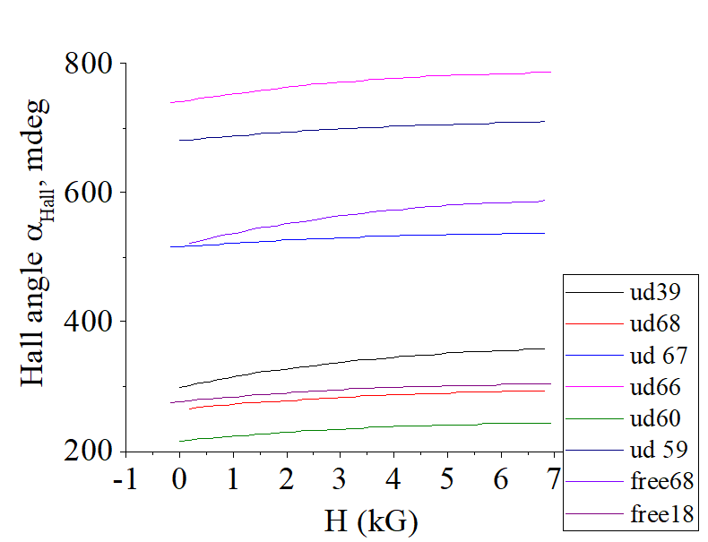
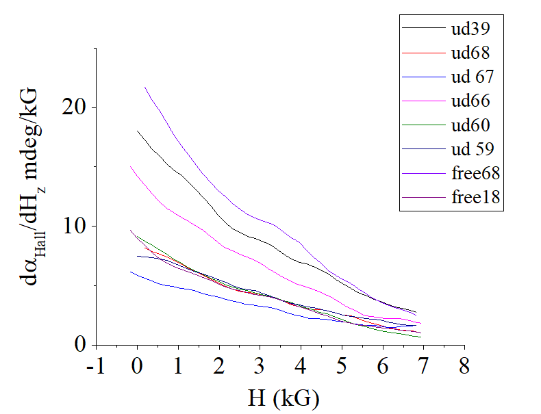
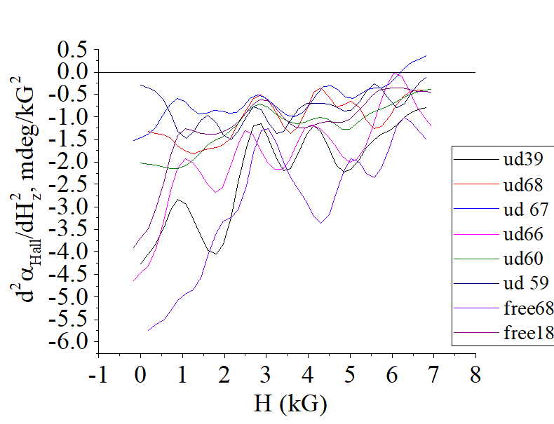
Hall angle, Anomalous Hall effect (AHE), Inverse Spin Hall effect (Sample dependence) |
|||||||||
|
|||||||||
details of this measurement method is here |
|||||||||
| Sample Volt53: Ta(2.5 nm)/ FeBCo(x=0.3, 1 nm) MgO(5.1 nm)/ Ta(1nm)/ Ru(5 nm) | |||||||||
| click on image to enlarge it |
The Hall angle αHall , its 1st derivation ∂αHall/∂Hz and its 2d derivation ∂2αHall/∂Hz2 is simultaneously fitted by equation (See here)
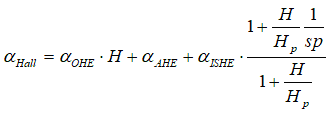
where αOHE is Hall angle of Ordinary Hall effect, αAHE is Hall angle of Anomalous Hall effect and where αISHE is Hall angle of Inverse Spin Hall effect
There is an ambiguity for αISHE and αAHE, which depends on unknown spin polarization sp
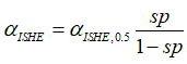
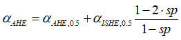
where sp is the spin polarization of conduction electrons, αAHE,0.5 is αAHE at sp=0.5, αISHE,0.5 is αISHE at sp=0.5
sample:( free68 gate) ![]() αISHE,0.5= 410 mdeg; αAHE,0.5=1401 mdeg; αOHE=0.2 mdeg/kG; Hp=4.73 kG;
αISHE,0.5= 410 mdeg; αAHE,0.5=1401 mdeg; αOHE=0.2 mdeg/kG; Hp=4.73 kG;
sample:( free18 gate) ![]() αISHE,0.5= 159 mdeg; αAHE,0.5=816 mdeg; αOHE=0.2 mdeg/kG; Hp=5.73 kG;
αISHE,0.5= 159 mdeg; αAHE,0.5=816 mdeg; αOHE=0.2 mdeg/kG; Hp=5.73 kG;
sample:( ud59) ![]() αISHE,0.5= 163 mdeg; αAHE,0.5=2225 mdeg; αOHE=0.2 mdeg/kG; Hp=5.84 kG;
αISHE,0.5= 163 mdeg; αAHE,0.5=2225 mdeg; αOHE=0.2 mdeg/kG; Hp=5.84 kG;
sample:( ud60) ![]() αISHE,0.5= 165 mdeg; αAHE,0.5=590 mdeg; αOHE=0.2 mdeg/kG; Hp=5.06 kG;
αISHE,0.5= 165 mdeg; αAHE,0.5=590 mdeg; αOHE=0.2 mdeg/kG; Hp=5.06 kG;
sample:( ud66) ![]() αISHE,0.5= 274 mdeg; αAHE,0.5=2324 mdeg; αOHE=0.2 mdeg/kG; Hp=5.84 kG;
αISHE,0.5= 274 mdeg; αAHE,0.5=2324 mdeg; αOHE=0.2 mdeg/kG; Hp=5.84 kG;
sample:( ud67) ![]() αISHE,0.5= 113 mdeg; αAHE,0.5=1677 mdeg; αOHE=0.2 mdeg/kG; Hp=6.01 kG;
αISHE,0.5= 113 mdeg; αAHE,0.5=1677 mdeg; αOHE=0.2 mdeg/kG; Hp=6.01 kG;
sample:( ud68) ![]() αISHE,0.5=162 mdeg; αAHE,0.5=767 mdeg; αOHE=0.2 mdeg/kG; Hp=4.91 kG;
αISHE,0.5=162 mdeg; αAHE,0.5=767 mdeg; αOHE=0.2 mdeg/kG; Hp=4.91 kG;
sample:( ud39) ![]() αISHE,0.5=392 mdeg; αAHE,0.5=657 mdeg; αOHE=0.2 mdeg/kG; Hp=6.18 kG;
αISHE,0.5=392 mdeg; αAHE,0.5=657 mdeg; αOHE=0.2 mdeg/kG; Hp=6.18 kG;
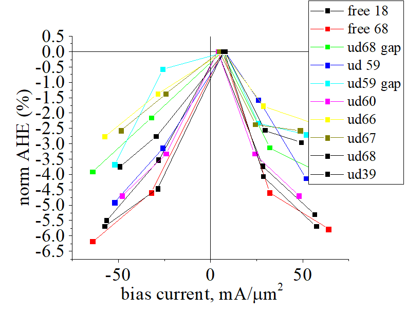
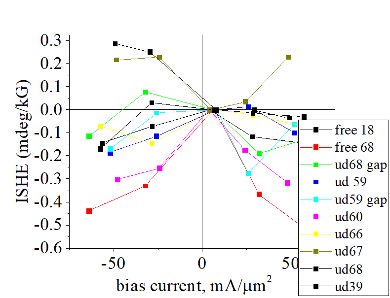
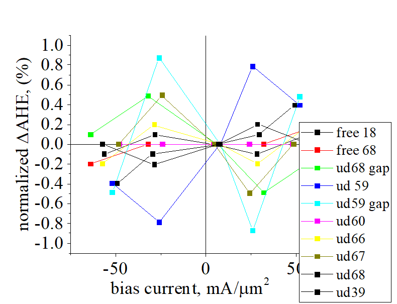
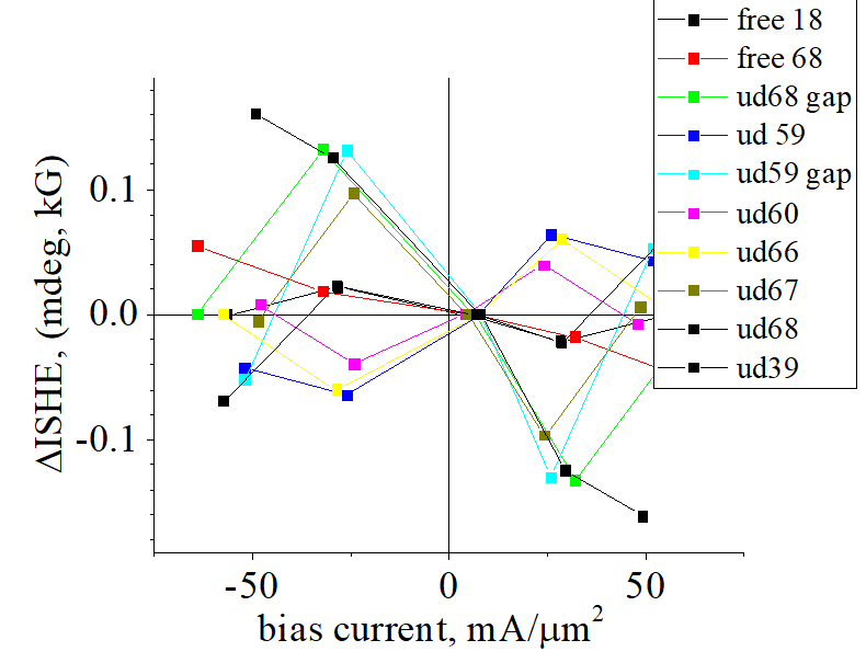
 AHE & ISHE
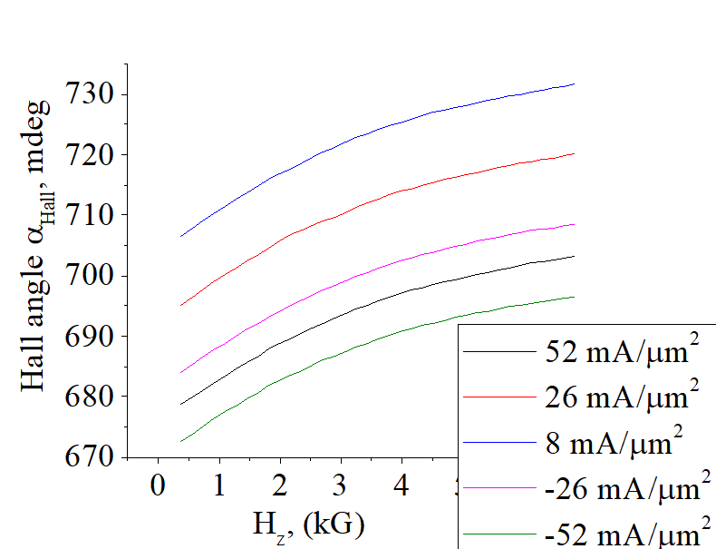
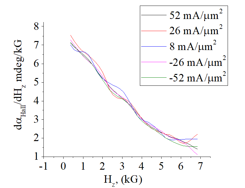
 Spin-orbit torque. Hall angle, Anomalous Hall effect (AHE), Inverse Spin Hall effect vs current |
||||||||||||||||||
|
||||||||||||||||||
details of this measurement method is here |
||||||||||||||||||
| Sample Volt53: Ta(2.5 nm)/ FeBCo(x=0.3, 1 nm) MgO(5.1 nm)/ Ta(1nm)/ Ru(5 nm) | ||||||||||||||||||
| click on image to enlarge it |
(temperature) ![]()
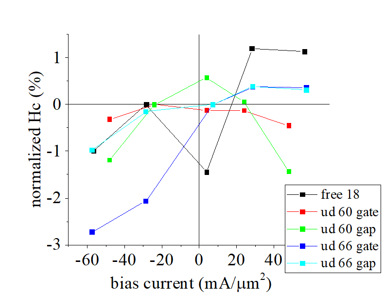
(AHE vs I2 ): strong 4-6 % decrease at current of 50 mA/ μm2; (fig.4a)
(ISHE vs I2 ):weak 0.2 mdeg/kG decrease at 50 mA/ μm2 (fig.4b)
(Spin- orbit torque) ![]()
(AHE(I)-AHE(-I)): moderate ~0.6-0.8 % ; slope: both negative & positive; saturation: at 50 mA/ μm2; (fig.4c)
(ISHE(I)-ISHE(-I)): very small (~0.1 mdeg/kG) (fig.4d)
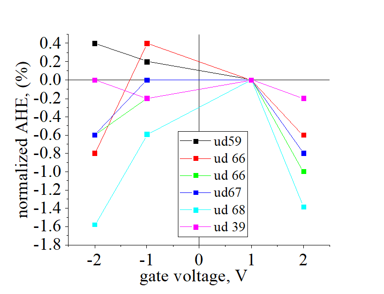
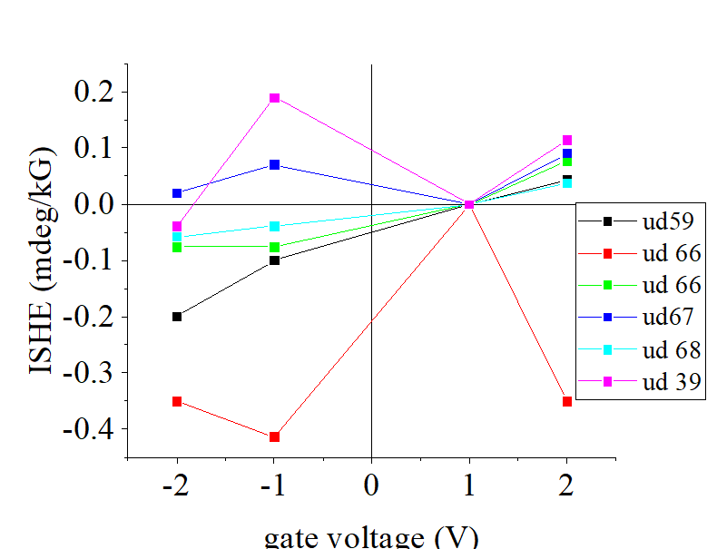
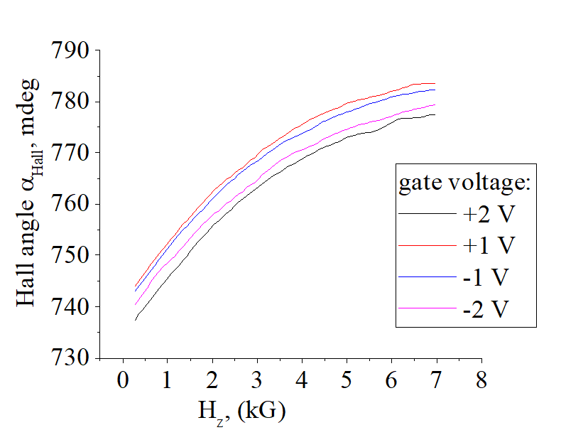
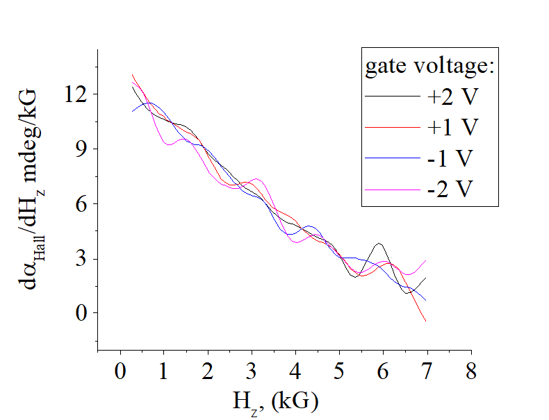
AHE & ISHE VCMA. Hall angle, Anomalous Hall effect (AHE), Inverse Spin Hall effect vs gate voltage |
||||||||||||
|
||||||||||||
details of this measurement method is here |
||||||||||||
| Sample Volt53: Ta(2.5 nm)/ FeBCo(x=0.3, 1 nm) MgO(5.1 nm)/ Ta(1nm)/ Ru(5 nm) | ||||||||||||
| click on image to enlarge it |
(AHE vs Vgate ): weak 0.4 % ; slope: unclear
(ISHE vs Vgate ): weak 0.2 mdeg/kG; slope: unclear
Measurement of PMA. Anisotropy field |
|||||||||
|
|||||||||
details of this measurement method is here |
|||||||||
| Sample Volt53: Ta(3 nm)/ FeB(1.1 nm)/ MgO(7 nm)/ W(1 nm) /Ru(5 nm) | |||||||||
| click on image to enlarge it |
Spin-orbit torque  vs PMA
Spin-orbit torque. Measurement of dependence of PMA on the electrical current j. |
||||||||||||
|
||||||||||||
details of this measurement method is here |
||||||||||||
| Sample Volt53: Ta(2.5 nm)/ FeBCo(x=0.3, 1 nm) MgO(5.1 nm)/ Ta(1nm)/ Ru(5 nm) | ||||||||||||
| click on image to enlarge it |
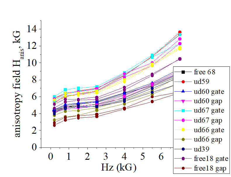
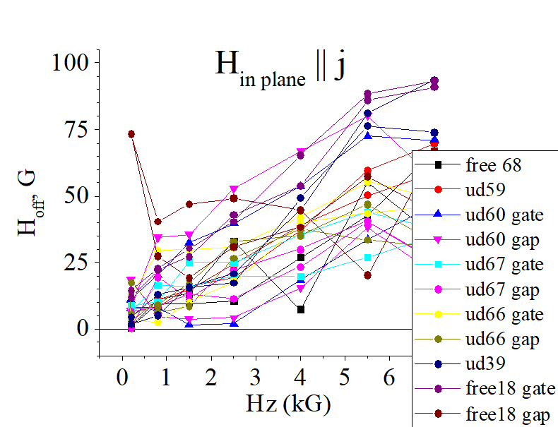
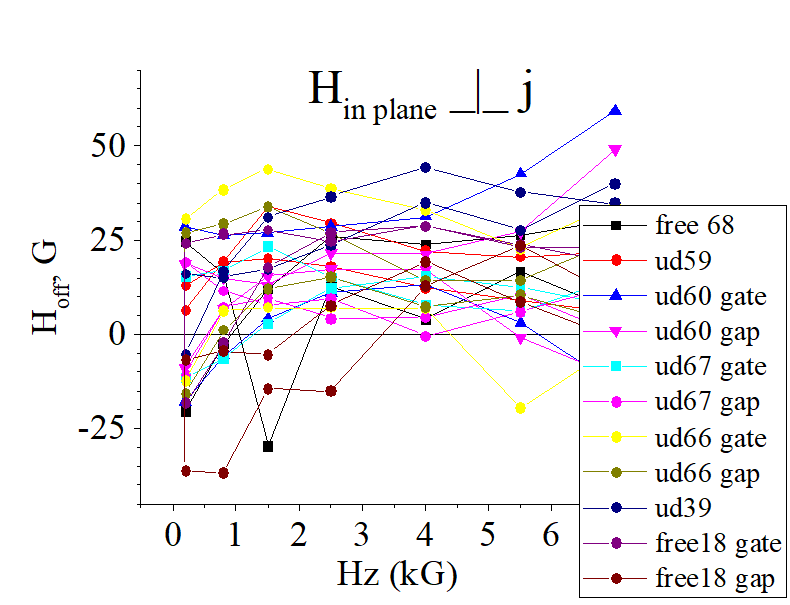
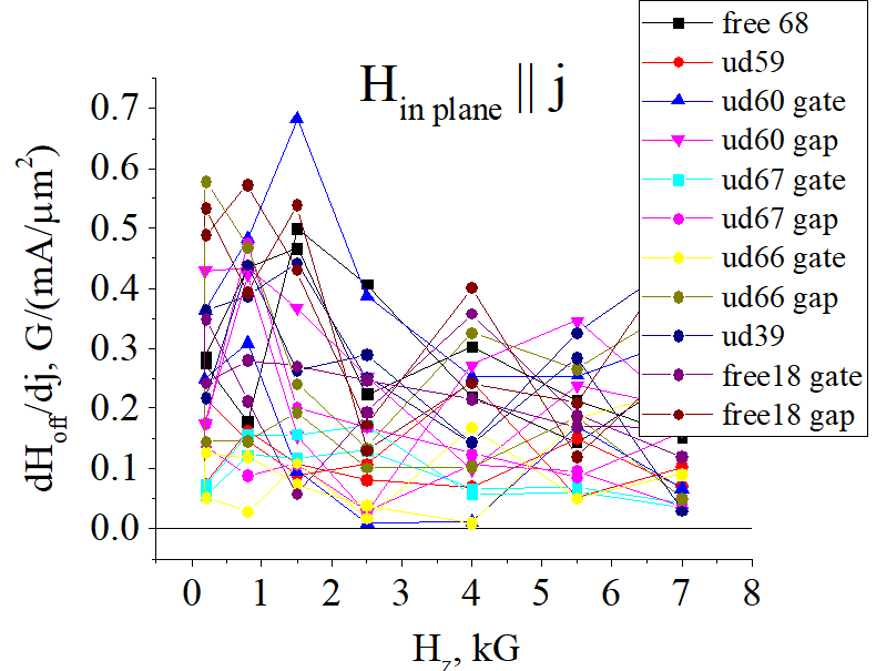
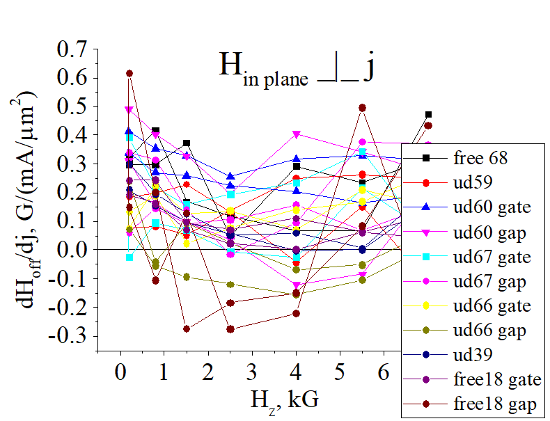
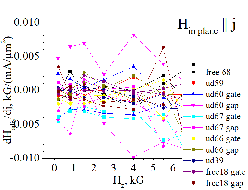
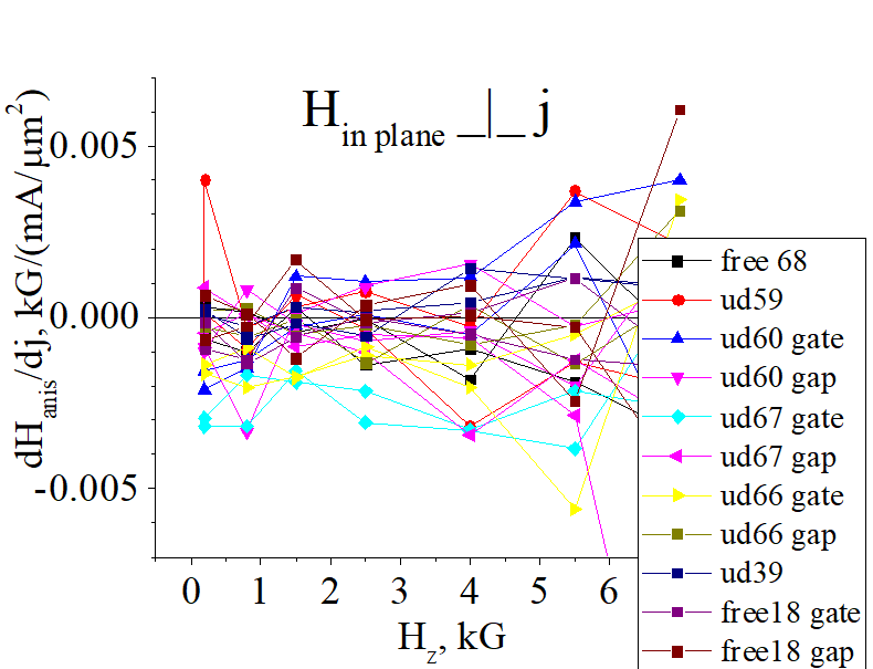
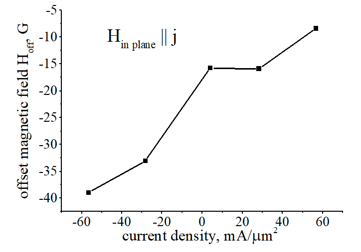
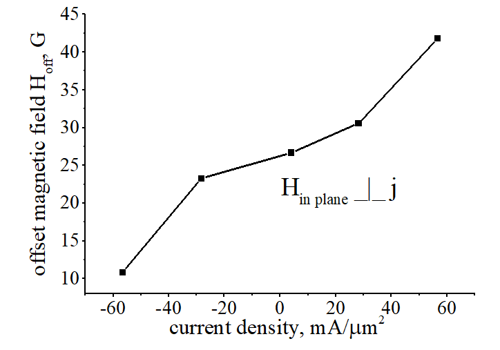
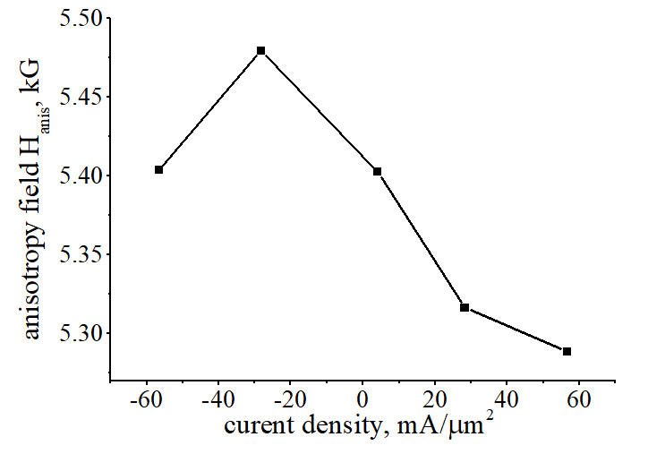
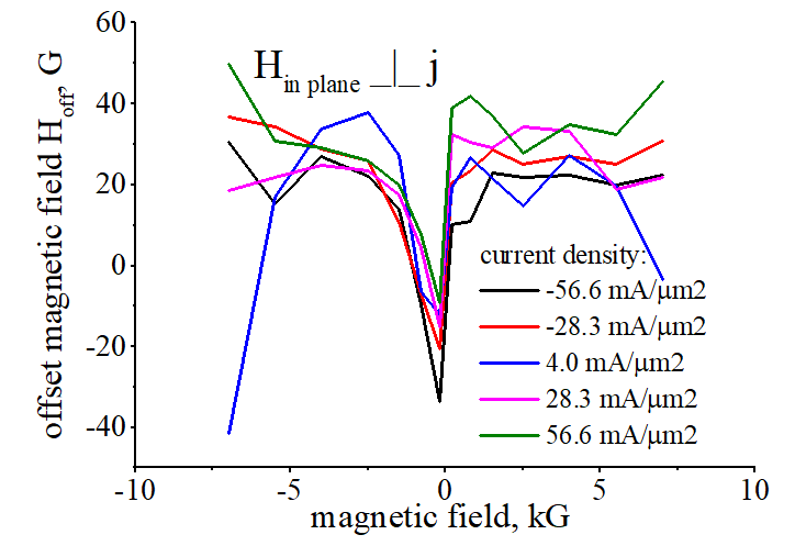
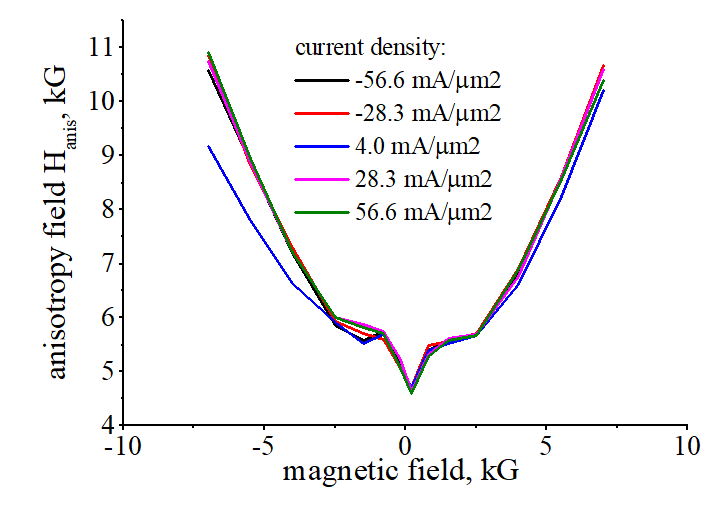
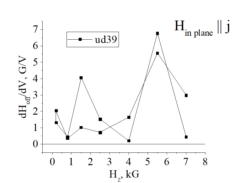
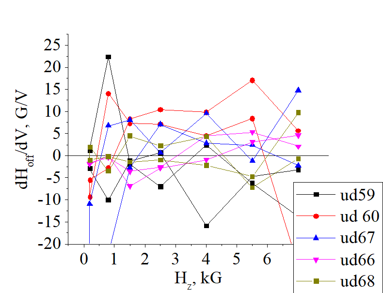
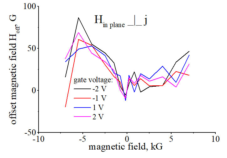
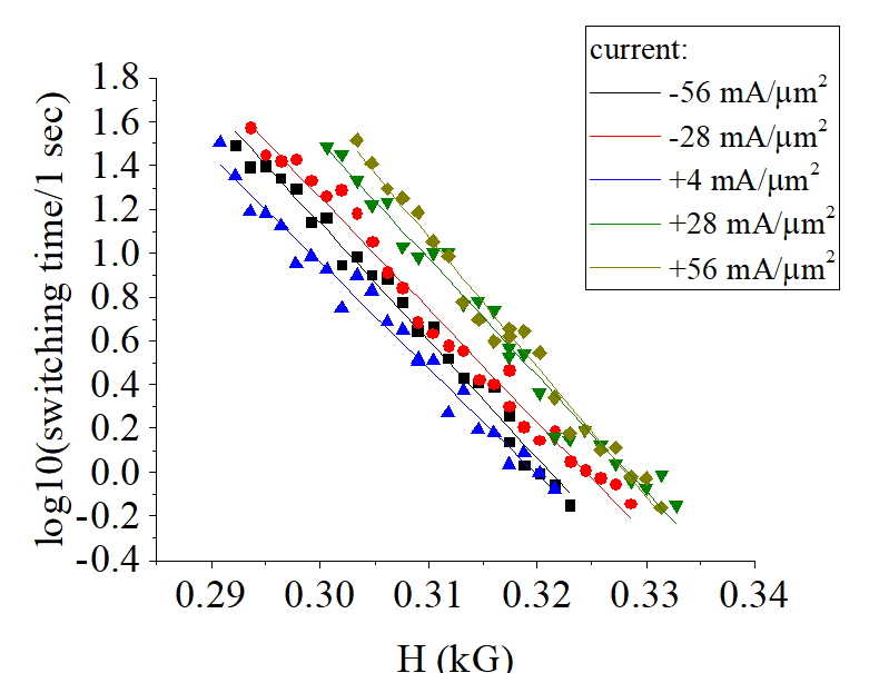
Spin-orbit torque. Measurement of dependence of anisotropy field Hanis and offset magnetic field Hoff on the electrical current j. |
||||||||||||||||||
|
||||||||||||||||||
Data of Sample free18 gate |
||||||||||||||||||
| details of this measurement method is here | ||||||||||||||||||
| click on image to enlarge it |
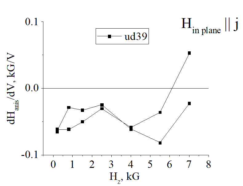
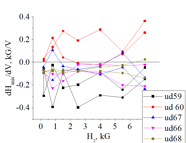
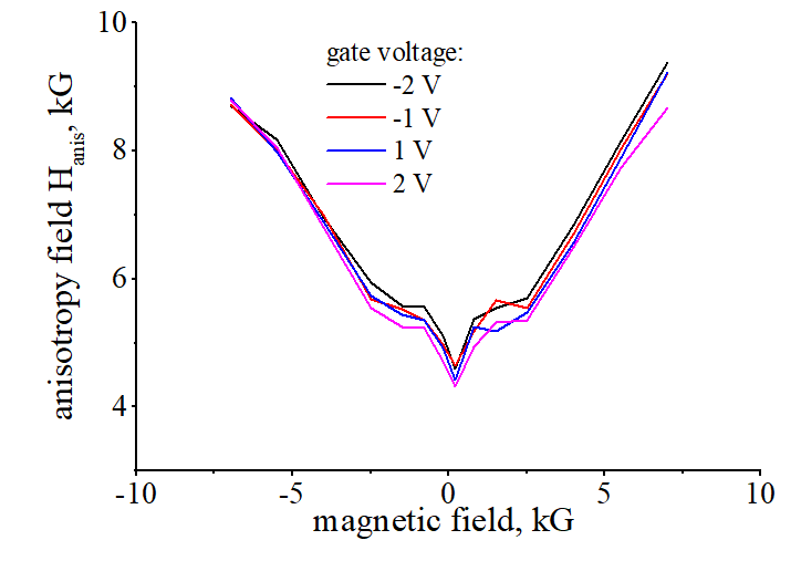
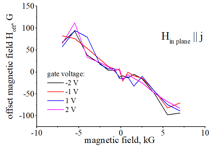
VCMA
VCMA. Measurement of dependence of PMA on gate voltage |
||||||||||||
|
||||||||||||
details of this measurement method is here |
||||||||||||
| Sample Volt53: Ta(2.5 nm)/ FeBCo(x=0.3, 1 nm) MgO(5.1 nm)/ Ta(1nm)/ Ru(5 nm) | ||||||||||||
| click on image to enlarge it |
Voltage-controlled magnetic anisotropy (VCMA). |
||||||||||||||||||
|
||||||||||||||||||
Data of Sample ud68 |
||||||||||||||||||
| details of this measurement method is here | ||||||||||||||||||
| click on image to enlarge it |
 Measurement of magnetization switching under external perpendicular magnetic field Hz
 SOT effect. Current dependence of magnetization switching parameters. |
|||||||||||||||||||||||||||
|
|||||||||||||||||||||||||||
details of this measurement method is here |
|||||||||||||||||||||||||||
| Sample Volt53: Ta(2.5 nm)/ FeBCo(x=0.3, 1 nm) MgO(5.1 nm)/ Ta(1nm)/ Ru(5 nm) | |||||||||||||||||||||||||||
| click on image to enlarge it |
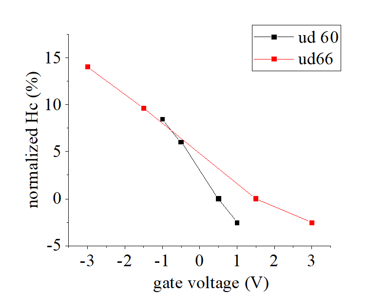
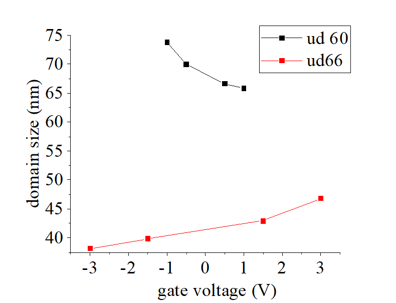
VCMA
VCMA. Measurement of dependence of PMA on gate voltage. |
||||||
|
||||||
details of this measurement method is here |
||||||
| Sample Volt53: Ta(2.5 nm)/ FeBCo(x=0.3, 1 nm) MgO(5.1 nm)/ Ta(1nm)/ Ru(5 nm) | ||||||
| click on image to enlarge it |
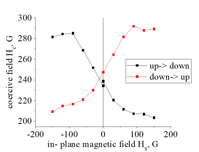
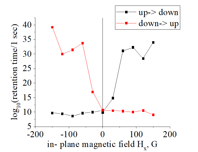
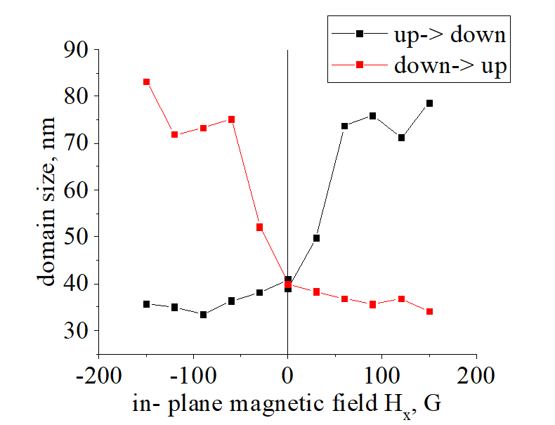
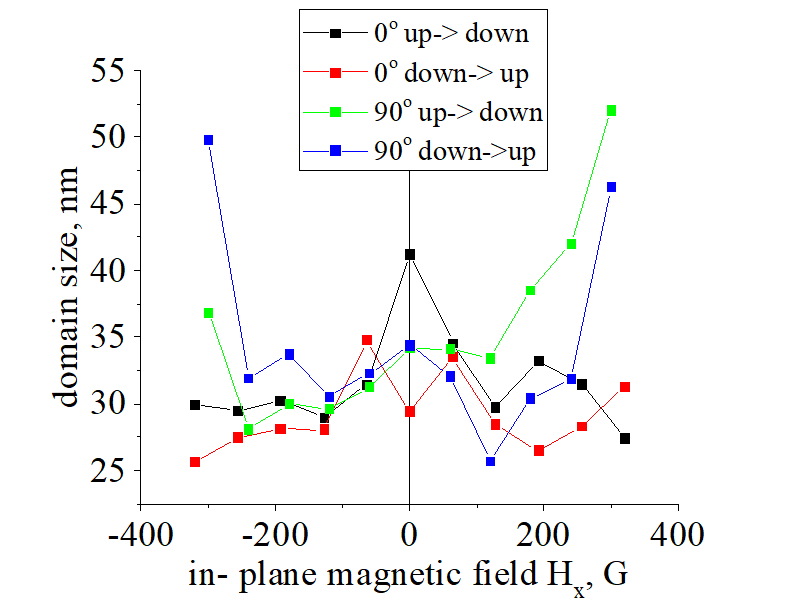
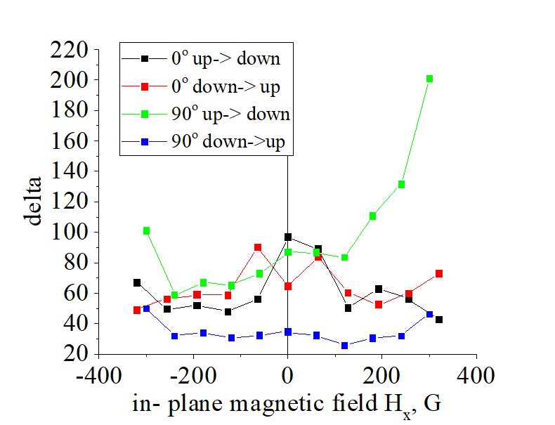
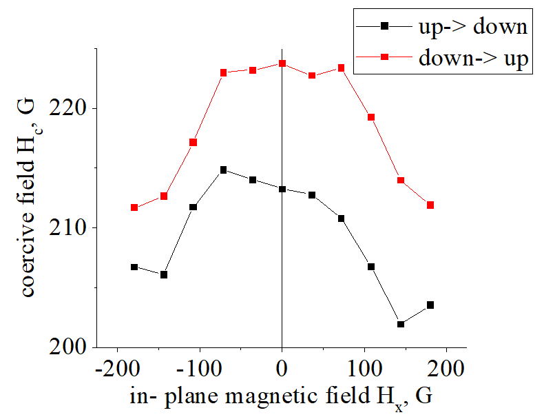
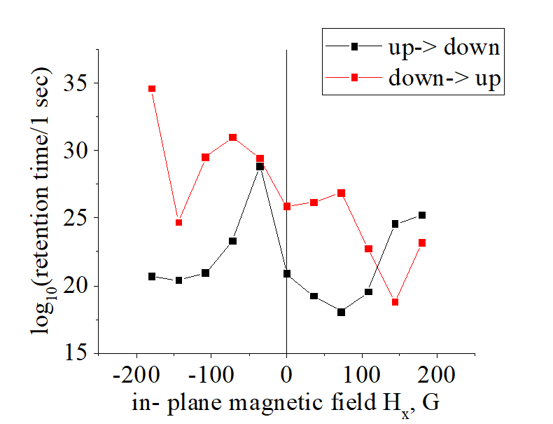
(fact 1) ![]() All parameters of thermo-activated switching (e.g. coercive field, retention time, parameter delta, size of nucleation domain) change substantially under external in-plane magnetic field Hx. There are several mechanisms for such change
All parameters of thermo-activated switching (e.g. coercive field, retention time, parameter delta, size of nucleation domain) change substantially under external in-plane magnetic field Hx. There are several mechanisms for such change
(mechanism 1: major) ![]() The size Hx on nucleation domain changes under Hx.
The size Hx on nucleation domain changes under Hx.
(mechanism 2: minor) ![]() The PMA energy EPMA on and therefore the energy barrier for the switching change under Hx.
The PMA energy EPMA on and therefore the energy barrier for the switching change under Hx.
(fact 2) ![]() The influence of in-plane magnetic field on switching parameters depends strongly on the number and distribution of fabricated defects and border irregularities in the nanomagnet. It makes the dependencies on Hx very different for nearly the same nanomagnets fabricated on same part of the same wafer.
The influence of in-plane magnetic field on switching parameters depends strongly on the number and distribution of fabricated defects and border irregularities in the nanomagnet. It makes the dependencies on Hx very different for nearly the same nanomagnets fabricated on same part of the same wafer.
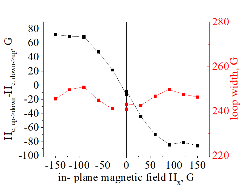
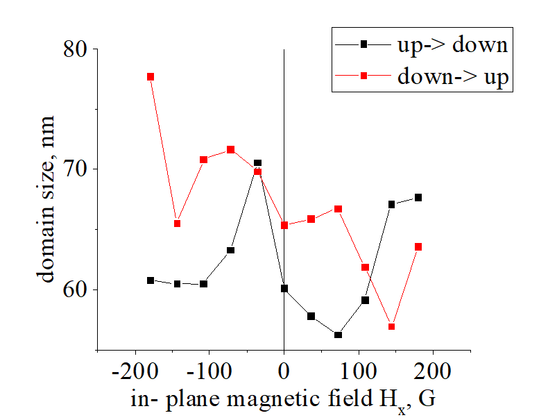
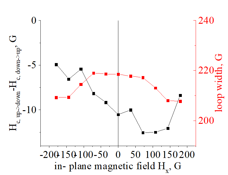
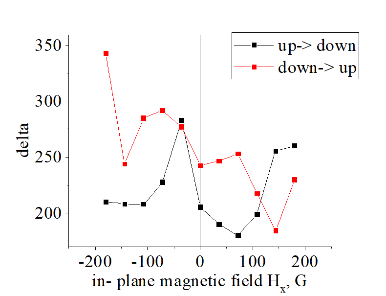
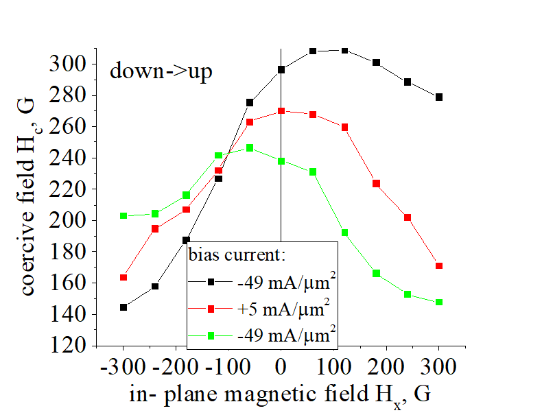
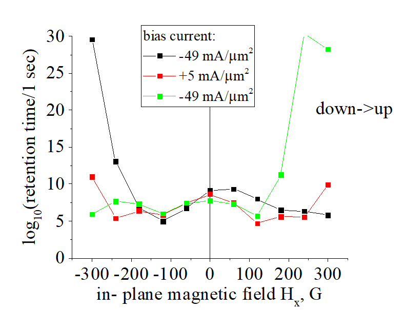
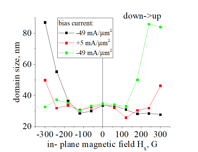
magnetization switching parameters under in-plane bias magnetic field Hx |
||||||||||||||||||
(up->down) corresponds to magnetization switching from up to down direction (left part of hysteresis loop); (down->up) corresponds to magnetization switching from down to up direction (right part of hysteresis loop); |
||||||||||||||||||
|
||||||||||||||||||
| details of this measurement method is here | ||||||||||||||||||
| device ud66, in-plane magnetic filed Hx is applied along current (Hx || to current: 0 deg) | ||||||||||||||||||
| click on image to enlarge it |
Coercive field
magnetization switching parameters under in-plane bias magnetic field Hx |
||||||||||||||||
(up->down) corresponds to magnetization switching from up to down direction (left part of hysteresis loop); (down->up) corresponds to magnetization switching from down to up direction (right part of hysteresis loop); |
||||||||||||||||
|
||||||||||||||||
| details of this measurement method is here | ||||||||||||||||
| Sample ud67 | ||||||||||||||||
| click on image to enlarge it |
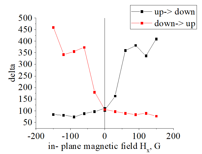
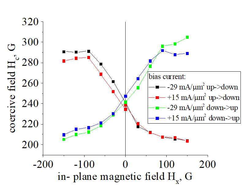
magnetization switching parameters under in-plane bias magnetic field Hx |
||||||||||||||||||
(up->down) corresponds to magnetization switching from up to down direction (left part of hysteresis loop); (down->up) corresponds to magnetization switching from down to up direction (right part of hysteresis loop); |
||||||||||||||||||
|
||||||||||||||||||
| details of this measurement method is here | ||||||||||||||||||
| Sample ud60, in-plane magnetic filed Hx is applied along current (Hx || to current: 0 deg) | ||||||||||||||||||
| click on image to enlarge it |
![]() Device ud67
Device ud67
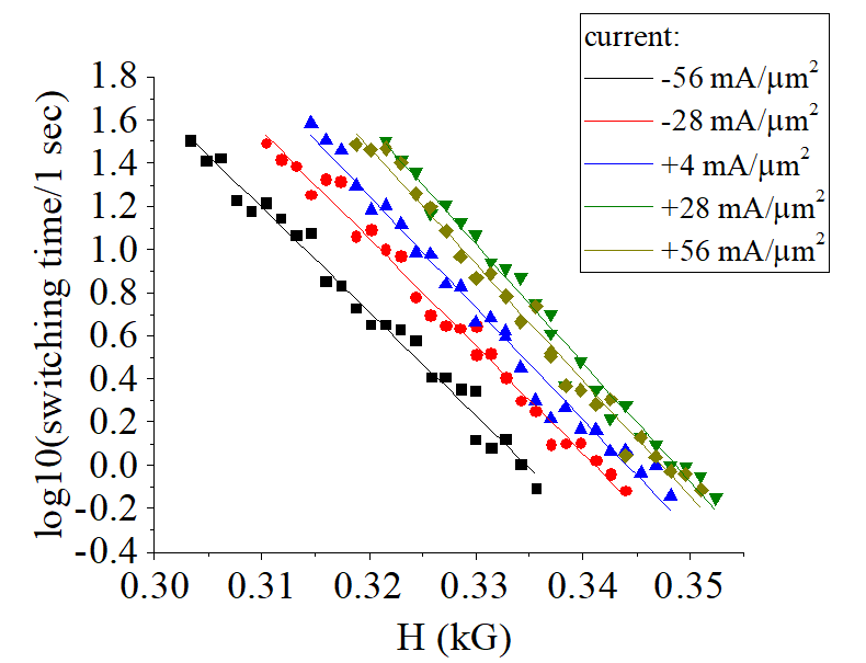
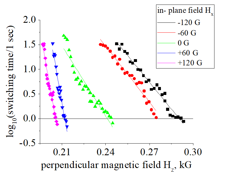
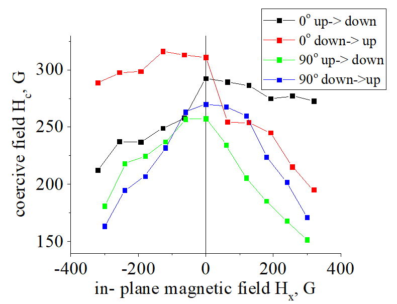
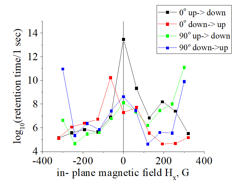
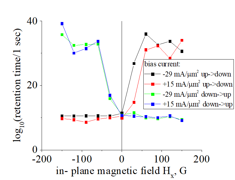
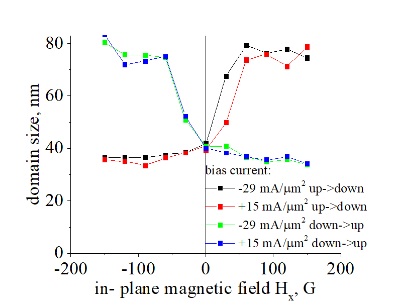
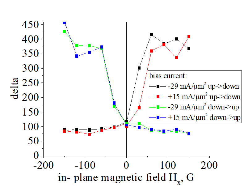
Current- dependence. SOT effect. Magnetization switching parameters under in-plane bias magnetic field Hx |
||||||||||||
(up->down) corresponds to magnetization switching from up to down direction (left part of hysteresis loop); (down->up) corresponds to magnetization switching from down to up direction (right part of hysteresis loop); |
||||||||||||
|
||||||||||||
| details of this measurement method is here | ||||||||||||
| Sample ud67, in-plane magnetic filed Hx is applied perpendicularly to current (Hx _|_ to current: 90 deg) | ||||||||||||
| click on image to enlarge it |
![]() Device ud66
Device ud66
Current- dependence. SOT effect. Magnetization switching parameters under in-plane bias magnetic field Hx |
||||||||||||
(up->down) corresponds to magnetization switching from up to down direction (left part of hysteresis loop); (down->up) corresponds to magnetization switching from down to up direction (right part of hysteresis loop); |
||||||||||||
|
||||||||||||
| details of this measurement method is here | ||||||||||||
| Sample ud67, in-plane magnetic filed Hx is applied along current (Hx || to current: 0 deg). V=2 V correspond | ||||||||||||
| click on image to enlarge it |
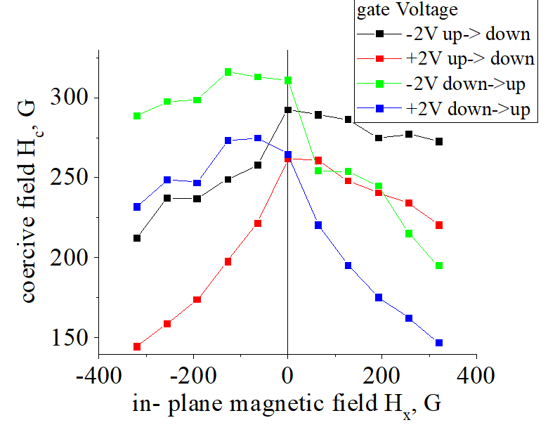
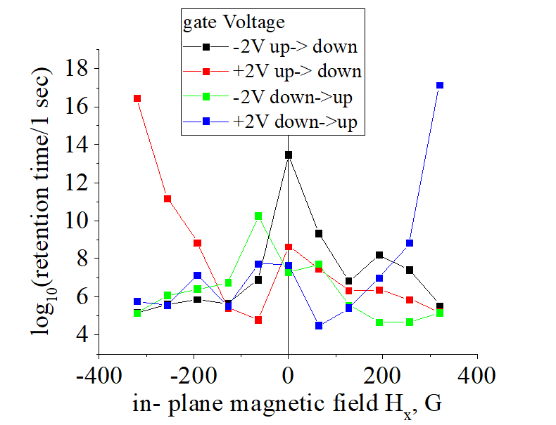
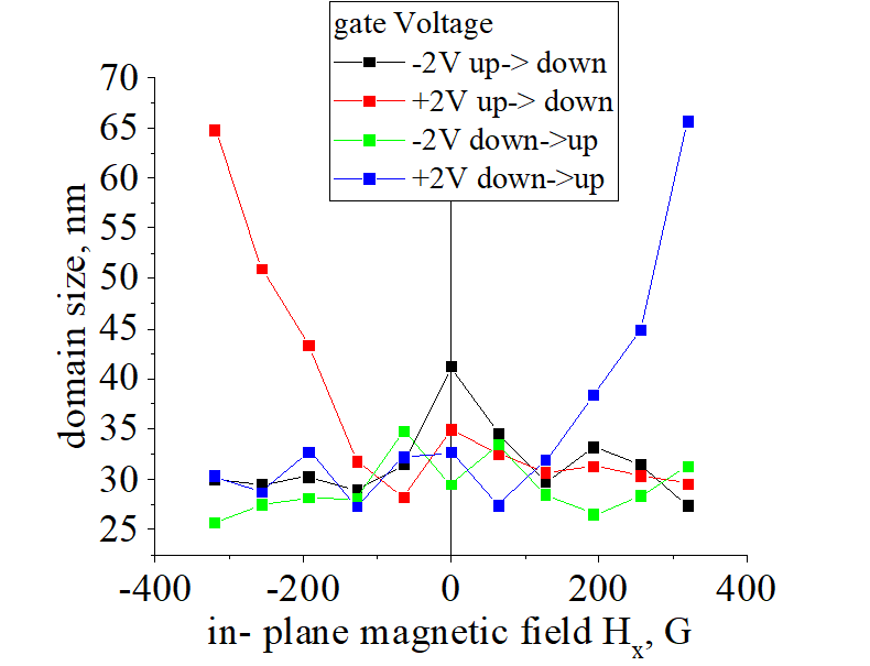
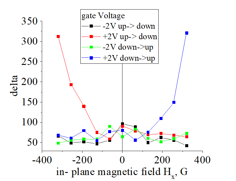
Dependence on a gate voltage. VCMA effect. Magnetization switching parameters under in-plane bias magnetic field Hx |
||||||||||||
(up->down) corresponds to magnetization switching from up to down direction (left part of hysteresis loop); (down->up) corresponds to magnetization switching from down to up direction (right part of hysteresis loop); |
||||||||||||
|
||||||||||||
| details of this measurement method is here | ||||||||||||
| Sample ud67, in-plane magnetic filed Hx is applied along current (Hx || to current: 0 deg) | ||||||||||||
| click on image to enlarge it |
![]()
![]() I am strongly against a fake and "highlight" research
I am strongly against a fake and "highlight" research ![]()
![]()
![]()
![]()
![]()
![]()
I will try to answer your questions as soon as possible
 Measurements