Dr. Vadym Zayets
v.zayets(at)gmail.com
My Research and Inventions
click here to see all content |

Dr. Vadym Zayetsv.zayets(at)gmail.com |
|
|
more Chapters on this topic:IntroductionTransport Eqs.Spin Proximity/ Spin InjectionSpin DetectionBoltzmann Eqs.Band currentScattering currentMean-free pathCurrent near InterfaceOrdinary Hall effectAnomalous Hall effect, AMR effectSpin-Orbit interactionSpin Hall effectNon-local Spin DetectionLandau -Lifshitz equationExchange interactionsp-d exchange interactionCoercive fieldPerpendicular magnetic anisotropy (PMA)Voltage- controlled magnetism (VCMA effect)All-metal transistorSpin-orbit torque (SO torque)What is a hole?spin polarizationCharge accumulationMgO-based MTJMagneto-opticsSpin vs Orbital momentWhat is the Spin?model comparisonQuestions & AnswersEB nanotechnologyReticle 11
|
All-optical Magnetization Switching Spin and Charge TransportAbstract:The all- optical magnetization switching describes the effect of the magnetization reversal of a ferromagnetic material when light illuminates it. Since a ferromagnetic material has two stable magnetization states, the data encoded in an optical pulse is memorized within the ferromagnetic material. All-optical magnetization switching can be used as a recording mechanism for ultra-high- speed optical memory.
|
| Magnetization reversal by light |
|---|
 |
| click on image to enlarge it |

![]() ..............
..............![]()
| All optical magnetization reversal | |||
|---|---|---|---|
|
|||
| the light, which is emitted by a laser, reverses the magnetization direction in the focusing spot | |||
| click on image to enlarge it |
The ultimate purpose of any optical data transmitting system is to send a data package from one memory chip to another memory chip. The larger the number of data can be sent in a shortest time interval, the better. A magnetic memory is a key memory for data processing. Using the all- optical magnetization switching it is possible to record data into the magnetic memory by a short optical pulse. Therefore, it might be possible that using the all- optical magnetization switching an effective high-speed optical memory can be made.

 |
 |
 |
| Part 1: Three mechanisms of all-optical magnetization switching | Part 2: High-speed Photon- to-Spin demultiplexing | Part 3: Efficiency of spin conversion from a photon to an electron. Search for a “magic” material |

There are 3 known mechanisms of the optical magnetization switching:
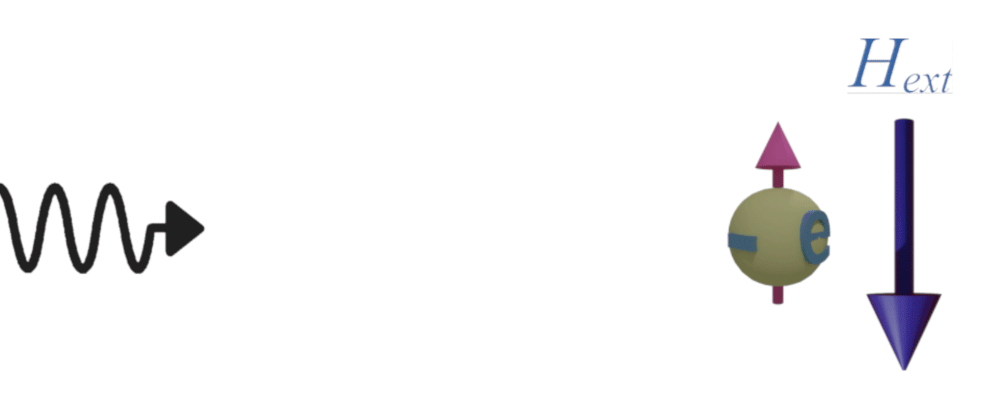
In the case a light pulse triggers the magnetization switching and the magnetization is reversed along the direction of an externally-applied magnetic field.
In the case the magnetization is switched up or down accordingly whether the polarization of the light pulse is left-circular or right- circular (accordingly to the Spin direction of a Photon)
In this case the magnetization is switched Into the opposite direction independently of the initial magnetization direction or the polarization of light .
|
|
| Magnetization switching assisted by an external magnetic field |
|---|
 |
 |
| For recording, a laser beam is focused into a very small spot on a magnetic disk and an external magnetic field is applied in the direction corresponding to the recorded data. For example, the magnetization up corresponds to the data "1" and the magnetization down corresponds to the data "0" |
| click on image to enlarge it |
This mechanism has been used for data recording in MO disks which were very popular as data storage about 10 years ago.
For recording, a laser beam is focused into a very small spot on a magnetic disk and an external magnetic field is applied in the direction corresponding to the recorded data. For example, the magnetization up corresponds to the data "1" and the magnetization down corresponds to the data "0"
The operation principle of this mechanism of of this mechanism of recording is based on heating of the recording area above the Curie temperature. As a result, the illuminated area is fully demagnetized, which means that each individual spins are directed in an absolutely random direction . Then, when the area is cooling down, the spins are aligned along the external magnetic field and the data is memorized.
| Physical mechanism. |
|---|
| of Magnetization switching assisted by an external magnetic field |
 |
| operation principle is based on heating of the recording area above the Curie temperature. |
| Under the heating of the optical pulse, the illuminated area is fully demagnetized, which means that each individual spins are directed in an absolutely random direction . Then, when the area is cooling down, the spins are aligned along the external magnetic field and the data is memorized. |
| click on image to enlarge it |
|
|
| Magnetization reversal by circular- polarized light (by Photons with Spin) |
|---|
|
|
| click on image to enlarge it |
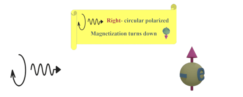
A circular- polarized photon has a Spin (momentum), which can be transferred into the Spin of electron reversing magnetization of a nanomagnet. As a result, the data encoded into the polarization of a photon is transformed into data encoded into the magnetization of a nanomagnet and, therefore, is memorized.
| Magnetization switching by a circularly polarized right |
|---|
 |
 |
| quarter wave plate is placed just below a laser, which has a linear polarization. Angle of the wave plate switches the polarization between left -circular, linear and right- circular. Magnetization is switched up or down accordingly whether the polarization of the light pulse is left-circular or right- circular. |
| when light polarization is right- circular, the spins under the focusing spot turn down. |
| linear polarization does not affects the spins |
| when light polarization is left- circular, the spins under the focusing spot turn up. |
| the left-circularly polarized light always switches the magnetization into up direction and the right -circularly polarized light always switches the magnetization down |
| click on image to enlarge it |
For this mechanism, the magnetization is switched up or down accordingly whether the polarization of the light pulse is left-circular or right- circular.
For example, the left-circularly polarized light always switches the magnetization into up direction and the right -circularly polarized light always switches the magnetization down independently of the initial magnetization direction.
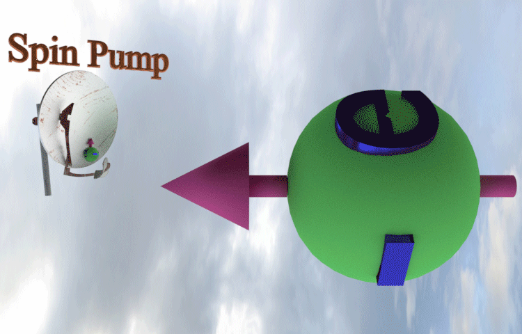
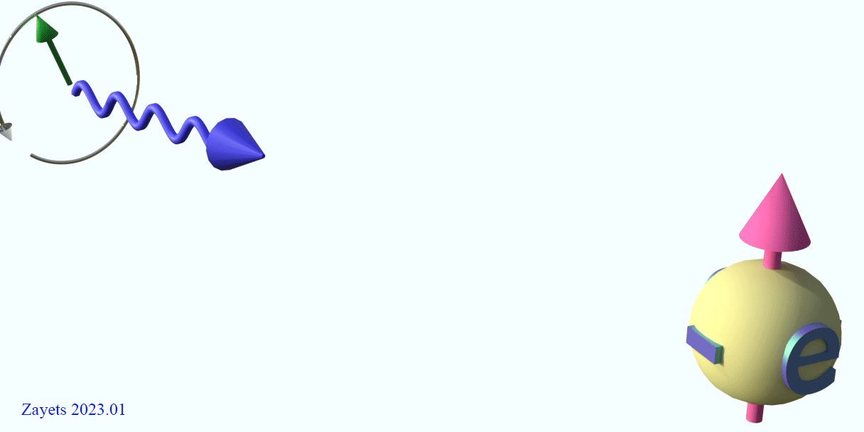
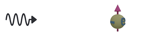
A circularly-polarized light has a momentum. A circularly-polarized photon has spin equal to either plus or minus 1. The spin of the photon transforms into the gas of the conduction electron polarizing the spins of the electrons in one direction or, the same, creating the spin-polarized conduction electrons.
The spin-polarized conduction electrons interact with the localized d- electrons turning their spin towards its own direction.
As a result, circularly- polarized photons turn the spins of the ferromagnetic material along its own direction.
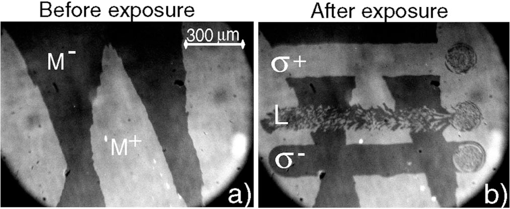
| Kerr image of a GdFeCo film. The darker area corresponds to the down direction of the magnetization and the whiter area corresponds to the up direction | ||||||||||||
|
||||||||||||
(result:) Right-circular-polarized light (σ+) turns the magnetization of film in the up- direction. Left-circular-polarized light (σ-) turns the magnetization in the down- direction. |
||||||||||||
|
||||||||||||
with a permission from Prof. A.V. Kimel (Radboud Uni.) |
||||||||||||
| click on image to enlarge it |
| Physical mechanism of Magnetization switching by a circularly polarized right |
|---|
 |
| click on image to enlarge it |
(how the momentum from light is transformed into the recorded data in a ferromagnetic material):
(step 1) A circularly polarized light is effectively absorbed by conduction electrons making the electron gas spin-polarized or if it was already spin-polarized, the light changes the direction and amount of the spin-polarization.
(step 2) The spins of the localized electrons turn along the spins of the conduction electrons, which leads to the reversal of the magnetization and the data recording.
| Path of how momentum of a photon is transformed to spin of a localized d-electron | |||||||||||||||||
|---|---|---|---|---|---|---|---|---|---|---|---|---|---|---|---|---|---|
| First, the momentum is transformed to the gas spin-polarized conduction electrons. Next, the momentum from the gas spin-polarized conduction electrons is transformed to the localized d-electrons. | |||||||||||||||||
|
|||||||||||||||||
| Fig.3. the path of how the momentum from light is transformed into the recorded data in a ferromagnetic material. | |||||||||||||||||
| click on image to enlarge it |
| Toggle Magnetization switching |
|---|
 |
 |
| click on image to enlarge it |
In this case of the toggle switching, the magnetization is switched Into the opposite direction independently of the initial magnetization direction and independently of the polarization of light .
It means that if the initial magnetization direction is up , the light pulse turns it to the down direction and if the initial magnetization direction is down, light switches it to the up direction.
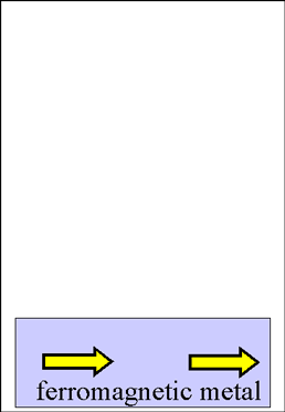
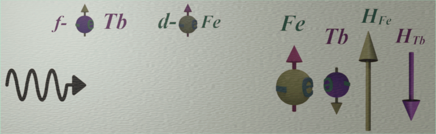
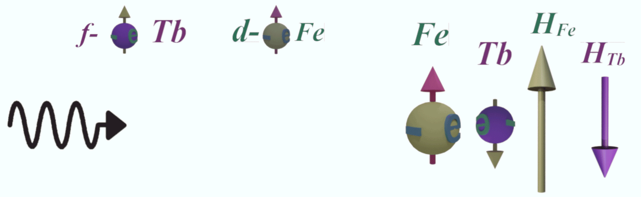
The toggle switching occurs in a compensated ferromagnets (e.g. FeTb). The localized electrons of Fe and Tb have different p- and f- symmetries. The exchange interaction is strong for similar electrons and weak for electrons of different symmetries. As a result, there is a very strong ferromagnetic exchange interaction between identical d- electrons of Fe and identical f- electrons of Tb. However, the antiferromagnetic exchange interaction between Fe and Tb is weak, even though the distances Fe-Fe, Tb-Tb and Fe-Tb are nearly the same in an amorphous FeTb.
In FeTb, photons mainly interact with conduction electrons, because of their comparable size. Heating of localized electrons is mainly due to their interaction with the hot conduction electrons. The sp- symmetry of conduction electrons is more similar to the d-symmetry of Fe than the f- symmetry of Tb. As a result, the Fe electrons are heated more efficiently than the Tb electrons.
In the case of the toggle switching, an optical pulse heats and demagnetizes only Fe magnetic lattice, while Tb lattice remains magnetized. When cooling, the Fe spins are aligned along the internal magnetic field, which at this moment is along the Tb spins. Later, the Tb spins are reversed to align antiferromagnetically with more numerous Fe spins. As a result, the magnetization is reversed to the opposite direction.
| Kerr image of a GdFeCo film. The darker area corresponds to the down direction of the magnetization and the whiter area corresponds to the up direction |
 |
| The upper row shows the case when initially the film is magnetized in the up direction. The 1st pulse turns the magnetization up, the 2nd turns it down, the 3rd turns it again up and so on. |
| The low row shows the case when initial magnetization direction is down. The 1st pulse turns the magnetization down, the 2nd turns it up, the 3rd turns it again down and so on. |
| (result:) When a laser illuminates the magnetic film, all spins within the focusing spot turn into the opposite direction. Next pulse turns the spins back and next pulse turns the spins opposite and so on. |
|
with a permission from Prof. A.V. Kimel (Radboud Uni.) |
| click on image to enlarge it |
If the 1st and the 2nd types of switching can occur in any ferromagnetic material like iron or cobalt, the toggle switching can occur only in a material, which is called the compensated ferromagnet.
The compensated ferromagnet like FeTb is a compound of two metals. Each metal has a different symmetry of the localized electron. For example, the symmetry of Fe electrons is the d- type and the symmetry of Tb electrons is the f- type. This material has two spin lattices. In each lattice all spins are aligned in one direction, There is a weak antiferromagnetic interaction between the Fe lattice and the Tb lattice. As a result, all spins of Tb electrons are opposite to the spins of Fe electrons. (See more details about exchange interaction here)
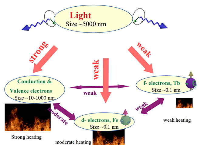
When light is focused on a material, it mainly interacts with the conduction and valence electrons. As a result, the temperature of the gas of conduction electrons increases substantially. Because of the moderate interaction of the d-electron and the conduction electrons, the temperature of d-electrons increases, but not as much as the temperature of the conduction electrons. There is some heating of the f- electrons, but it is very weak, because of very weak interaction of the f- electrons with both the conduction and d- electrons.
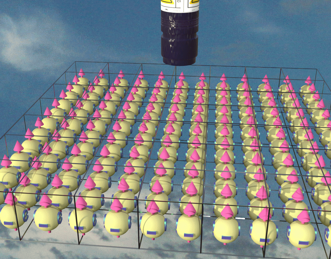
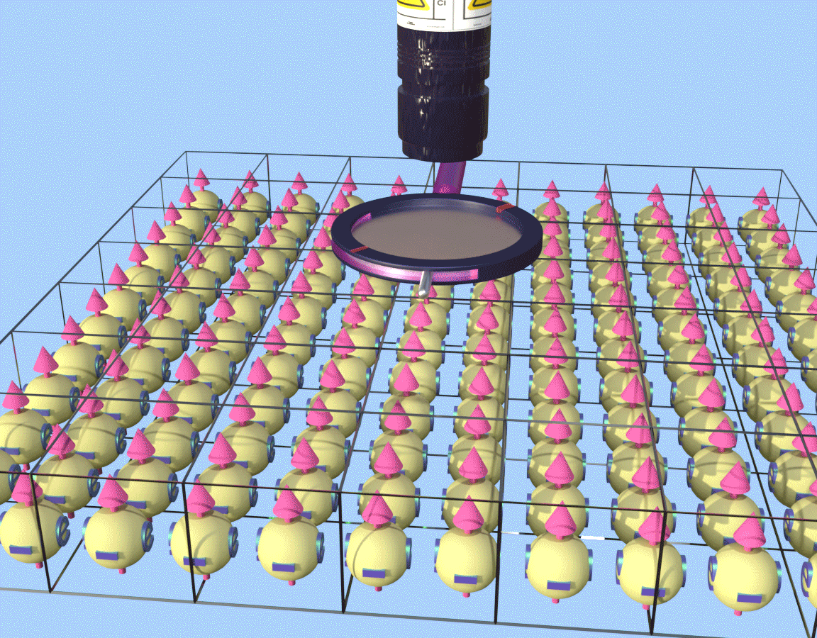
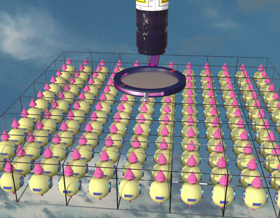
Compensated Ferromagnet: a material for a toggle switching |
|||||||||||
|---|---|---|---|---|---|---|---|---|---|---|---|
|
|||||||||||
| click on image to enlarge it |
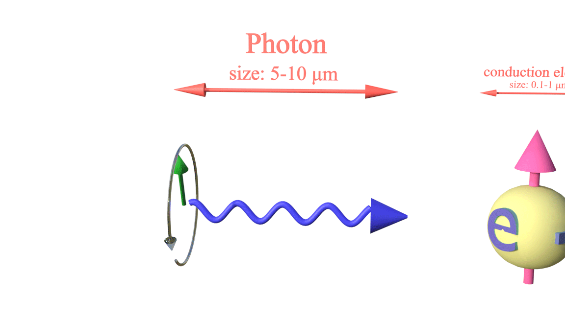
| The size is matter. |
|---|
 |
 |
| click on image to enlarge it |
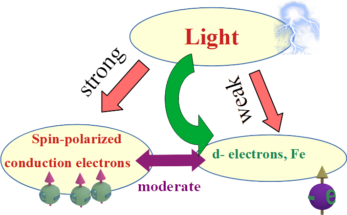
The size of a photon, which is focused into a small spot, is about 5um. The size of a conduction or valence electron is between 10 and 1000 nm depending on the crystal quality of a material. As a result, the light interaction with a conduction electron is strong and effective. The size of localized d- and f- electrons is about the orbital size, which is about 0.1 nm. As a result, the light interaction with d- and f- electrons is weak and inefficient.
This fact can be easily verified just by looking at the absorption spectrum of any material. The absorption due to the conduction and valence electrons is broad and strong. The narrow absorption peaks of d- or f- electrons are tiny and barely distinguished.

(fact): ![]() Scattering probability between two states of an electron is highest when the symmetries of both the initial state and the final state are similar.
Scattering probability between two states of an electron is highest when the symmetries of both the initial state and the final state are similar.
For this reason, ![]() the scattering probability is:
the scattering probability is:
(highest): between a conduction and a conduction electron
(moderate): between a conduction of p- symmetry and a localized d- electron
(weaker): between a conduction of s- symmetry and a localized d- electron
(weak): between a conduction and a localized f- electron
the heating ![]() is:
is:
(highest): for conduction electrons
(moderate): for localized d- electrons
(weak): for localized f- electrons
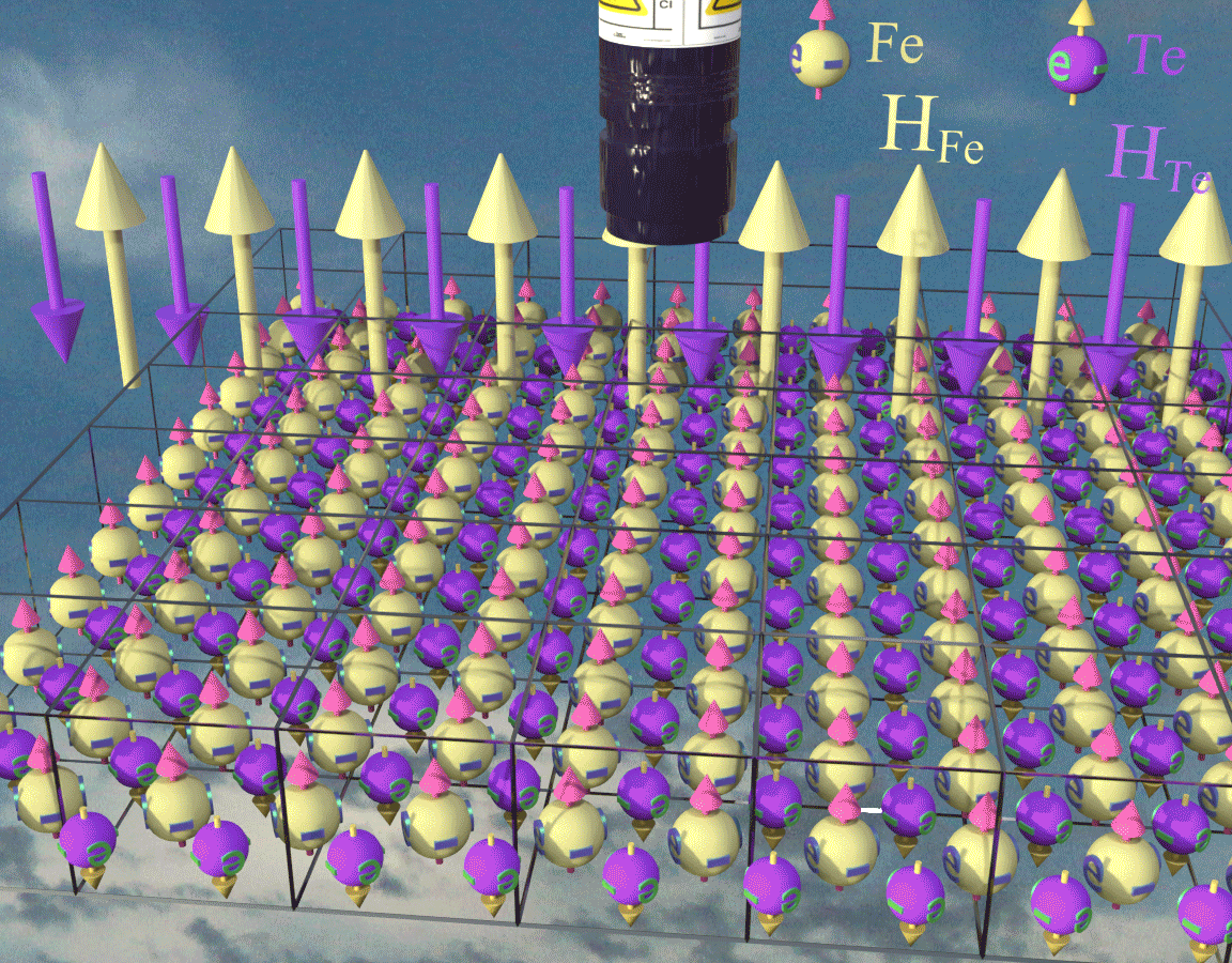
| Physical mechanism of Toggle switching . |
|---|
 |
| The green and purple balls show the Fe and Tb spins. The arrows show the intrinsic magnetic field along Fe spins and Tb spins. |
| A laser pulse demagnetizes the Fe spins meaning that the Fe spins are distributed in all directions, while Tb spins remain in one direction. During cooling the Fe spins are aligned along the magnetic field of Tb. Next, the Tb spins are rotated to be opposite to the direction of Fe spins. |
| click on image to enlarge it |
The FeTb consists of two spin system the Fe and Tb systems, which are antiferromagnetically coupled Along each spin system there is a magnetic field, which is shown by an arrow of corresponding color.. In an equilibrium two magnetic fields are opposite to each other.
The Light pulse is heating mainly the Fe spins almost without heating of Tb spins. As a result, the temperature of Fe electrons exceeds the Curie temperature and the Fe spins are demagnetized. In contrast, the Tb electrons remain cool and keep their spin direction. Consequently, the magnetic field along Fe spins vanishes and the magnetic field along Tb remains.
When Fe electrons are cooling down, their spins are aligned along the only-existed magnetic field, which is the Tb magnetic field. Therefore, the Fe spins are aligned parallel to the Tb spins. However, there is an antiferromagnetic exchange interaction between Fe and Tb electrons. Since there are more Fe atoms, the antiferromagnetic exchange turns the Tb spins to be opposite to the Fe spins.
In total, the optical pulse fully reverses the magnetization. The magnetization direction always changes to the opposite independently of its initial state.
| Physical mechanism of Toggle switching . |
|---|
 |
| animation shows how each spin behaves during the toggle switching. |
| The green and purple balls show the Fe and Tb spins. The arrows show the intrinsic magnetic field along Fe spins and Tb spins. |
| A laser pulse demagnetizes the Fe spins meaning that the Fe spins are distributed in all directions, while Tb spins remain in one direction. During cooling the Fe spins are aligned along the magnetic field of Tb. Next, the Tb spins are rotated to be opposite to the direction of Fe spins. |
| click on image to enlarge it |
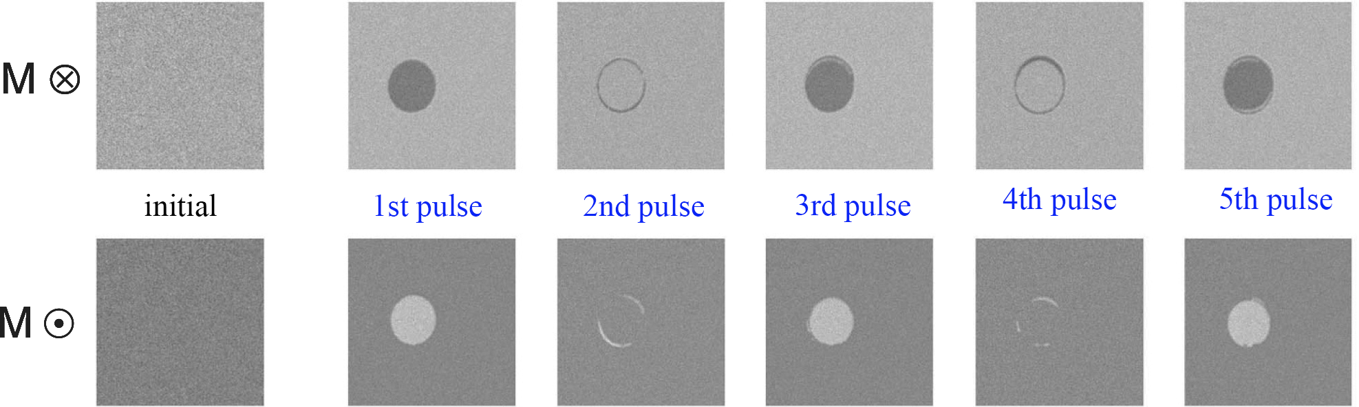
| Experimental verification of mechanism of toggle switching |
|---|
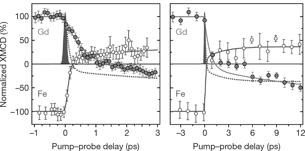
time evolution of the spins after a short optical pulse triggered a toggle switch in a GdFeCo film. |
| Time evolution of the spins of local electrons of Gd (filled circles) and Fe (empty circles) after illumination of a GdFeCo film by a femtosecond pulse. The perpendicular- to - plane component of the spin is proportional to the amplitude of the XMCD signal. |
| Two graphs show the same data but with a different time scale. |
(result:) The Fe spin is quickly demagnetized and next is aligned along the magnetic field of the Gd spins. The Gd spin is demagnetized only a little and next is aligned slowly opposite to the Fe spin. |
|
with a permission from Prof. A.V. Kimel (Radboud Uni.) |
| click on image to enlarge it |
(fact): The amplitude of the X- ray magnetic circular dichroism (XMCD) is proportional to the spin (magnetization) of localized electrons. Turning the X-Ray wavelength to absorption peak of a specific element, the spin of specific element can be evaluated.
The XMCD measures the difference in the X-ray absorption between left and right circularly polarized x-ray, which is proportional to the spin.
Turning X-ray wavelength to the absorption edge of the specific element, the spin direction of only this element is measured.
![]() Time evolution:
Time evolution:
![]() (delay=0): optical pulse arrived
(delay=0): optical pulse arrived
![]() (delay=0.5 ps): Fe is demagnetized. Gd magnetization decreased, but Gd is still magnetized and keeps its initial spin direction.
(delay=0.5 ps): Fe is demagnetized. Gd magnetization decreased, but Gd is still magnetized and keeps its initial spin direction.
![]() (delay= 0.8 ps) Fe is re- magnetized along magnetic field of Gd. The precession of Gd spin is started as the Gd spin is slowly reversing its magnetization opposite to that of Fe.
(delay= 0.8 ps) Fe is re- magnetized along magnetic field of Gd. The precession of Gd spin is started as the Gd spin is slowly reversing its magnetization opposite to that of Fe.
(result of measured of spin dynamic): The heating by an optical pulse is different for localized electrons of the d- symmetry (Fe) and f- symmetry (Gd). The element of the d- symmetry (Fe) is heated quickly and efficiently. As a result, the d- element is demagnetized. In contrast, the element of the f- symmetry (Gd) is heated only slightly and keeps its initial magnetization. During cooling, the element of the d- symmetry (Fe) is magnetized along magnetic field of Gd. Due to the antiferromagnetic coupling between Fe and Gd, the spin of Gd is reversed. The spin precession during the spin reversal can be observed.
| Conventional high-speed optical memory |
|---|
Optical memory=Photodetector +DRAM |
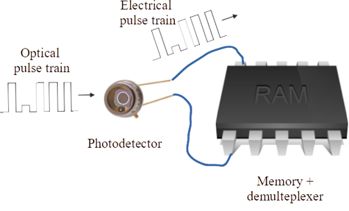 |
| In present high-speed optical data- processing circuits, the high-speed optical memory is made of a high-speed photo-detector and DRAM. |
The ultimate purpose of any optical data transmitting system is to send a data package from one memory chip to another memory chip. The larger the number of data can be sent in a shortest time interval, the better.
![]() A magnetic memory is a key memory for data processing. Using the all- optical magnetization switching it is possible to record data into the magnetic memory by a short optical pulse.
A magnetic memory is a key memory for data processing. Using the all- optical magnetization switching it is possible to record data into the magnetic memory by a short optical pulse.
it might be possible that the all- optical magnetization switching might be used as an ultra fast and effective recording mechanism for the high-speed optical memory.
 Conventional high-speed optical memory=Photodetector + electrical memory
(fact): ![]() The parameters of a possible new memory, which would be based on the effect of the all- optical magnetization switching, should be at least comparable and hopefully better than this already-existed high-speed optical memory.
The parameters of a possible new memory, which would be based on the effect of the all- optical magnetization switching, should be at least comparable and hopefully better than this already-existed high-speed optical memory.
At present, high-speed optical memory is made by combining two components: a high-speed photodetector, which converts a train of optical pulses into a train of electrical pulses, and conventional electrical memory, like DRAM memory.
![]() The speed of the photodetector is larger than 100 GHz meaning it converts pulses with a period as small as 10 picoseconds. The clock frequency of advanced DRAM memory can be as fast as 10 GHz.
The speed of the photodetector is larger than 100 GHz meaning it converts pulses with a period as small as 10 picoseconds. The clock frequency of advanced DRAM memory can be as fast as 10 GHz.
![]() Additionally, the photodetectors, electrical demultiplexer, electrical data processor and DRAM memory can be integrated into one very- small chip.
Additionally, the photodetectors, electrical demultiplexer, electrical data processor and DRAM memory can be integrated into one very- small chip.
(main requirement): ![]() the recording speed of a new optical memory should be faster than the recording speed of an already- used optical memory.
the recording speed of a new optical memory should be faster than the recording speed of an already- used optical memory.
Importance of demultiplexing
Additionally to the storage of data,the demultiplexing (see below) is another very important function of high-speed optical memory
(Feasibility of method 1: the switching assisted by an external magnetic field): Low ![]()
This mechanism is based on heating of the ferromagnetic metal and, therefore, cannot be fast .
The heating due to the absorption of the optical pulse destroys magnetization of the ferromagnet. When the ferromagnet is cooled, its magnetization is aligned along the external magnetic field.
![]() The heating and cooling are famously slow processes.
The heating and cooling are famously slow processes. ![]() The fastest time scale of cooling is a few microseconds and the high-speed memory needs to operate a million times faster in a time scale of a few picoseconds.
The fastest time scale of cooling is a few microseconds and the high-speed memory needs to operate a million times faster in a time scale of a few picoseconds.
(Feasibility of method 2: toggle switching ): Low & moderate ![]()
Even though the origin of the toggled switching is more complex and fancy, still this mechanism is based on heating of the ferromagnetic metal and, therefore, cannot be fast. In the case of the toggled switching, only one of two magnetic lattices is heated by the optical pulse and destroyed.. During cooling, the magnetization of this lattice is aligned along the internal magnetic field.
In fact, this mechanism is very similar to the 1st mechanism. Only difference is that in the 1st mechanism the cooling and alignment occurs in a external magnetic field, but in the 2nd mechanism the cooling and alignment occurs in the internal magnetic field
![]() Similar to the 1st mechanism, the long time scale of the cooling limits the recording speed of this mechanism.
Similar to the 1st mechanism, the long time scale of the cooling limits the recording speed of this mechanism. ![]()
It is very unlikely that this recording mechanism of the toggled switching could be used in a high- speed memory, because of its slow speed.. The recording speed of combination the detector plus DRAM is faster and, therefore, a better and simpler solution for optical memory.
(Feasibility of method 3: Photon- to- Spin conversion): high 
The 3rd optical-recording mechanism is based on a transfer of the angular momentum from light to spins. Since it does not require any heating or cooling, the mechanism is fast.
. This mechanism is not averagely fast, but very fast (See details below)
![]()
![]()
![]()
![]()
Feasibility of High-speed recording using all-optical magnetization switching |
||||||||||||||||||||||||||||||||||||||||
|---|---|---|---|---|---|---|---|---|---|---|---|---|---|---|---|---|---|---|---|---|---|---|---|---|---|---|---|---|---|---|---|---|---|---|---|---|---|---|---|---|
|
||||||||||||||||||||||||||||||||||||||||
| click on image to enlarge it |
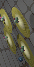
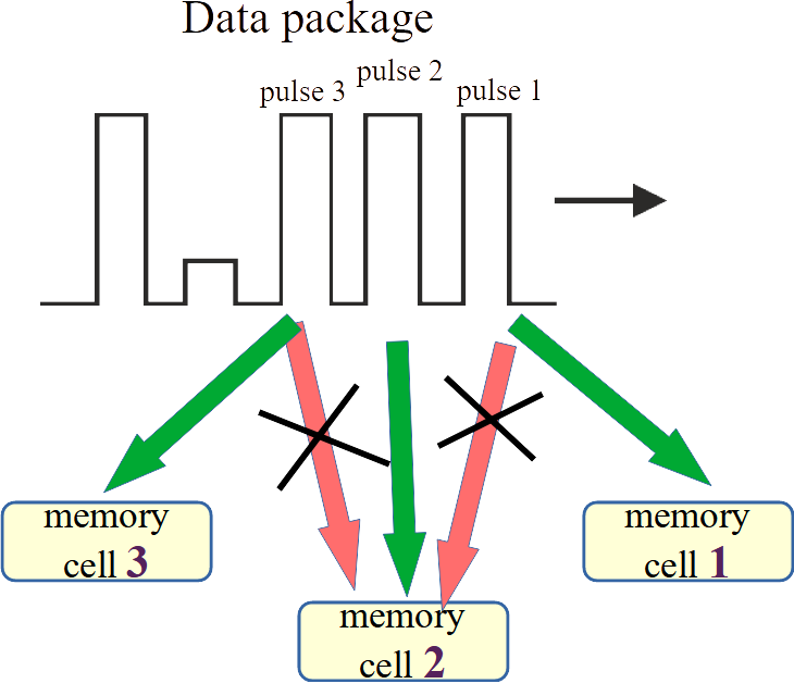
| Demultiplexing of a train of optical data pulses |
|---|
| demultiplexing means that each data of a train of short data pulses should be recorded to an individual memory cell. |
| the pulse number one should be recorded into the memory cell number one, the pulse number 2 should be recorded into the memory cell number two and so on. |
| neither the proceeding nor the following pulse should have any influence on the recorded data. Pulse N1 and pulse N3 should have no effect on the data recorded in memory cell 2. |
| click on image to enlarge it |
 Dumpling: a key function of any memory
 It is critically important that neither the proceeding nor the following pulse should have any influence on the recorded data.
Considering that the interval between pulses is extremely short, it is not a simple task and this high-speed task is done by a demultiplexer
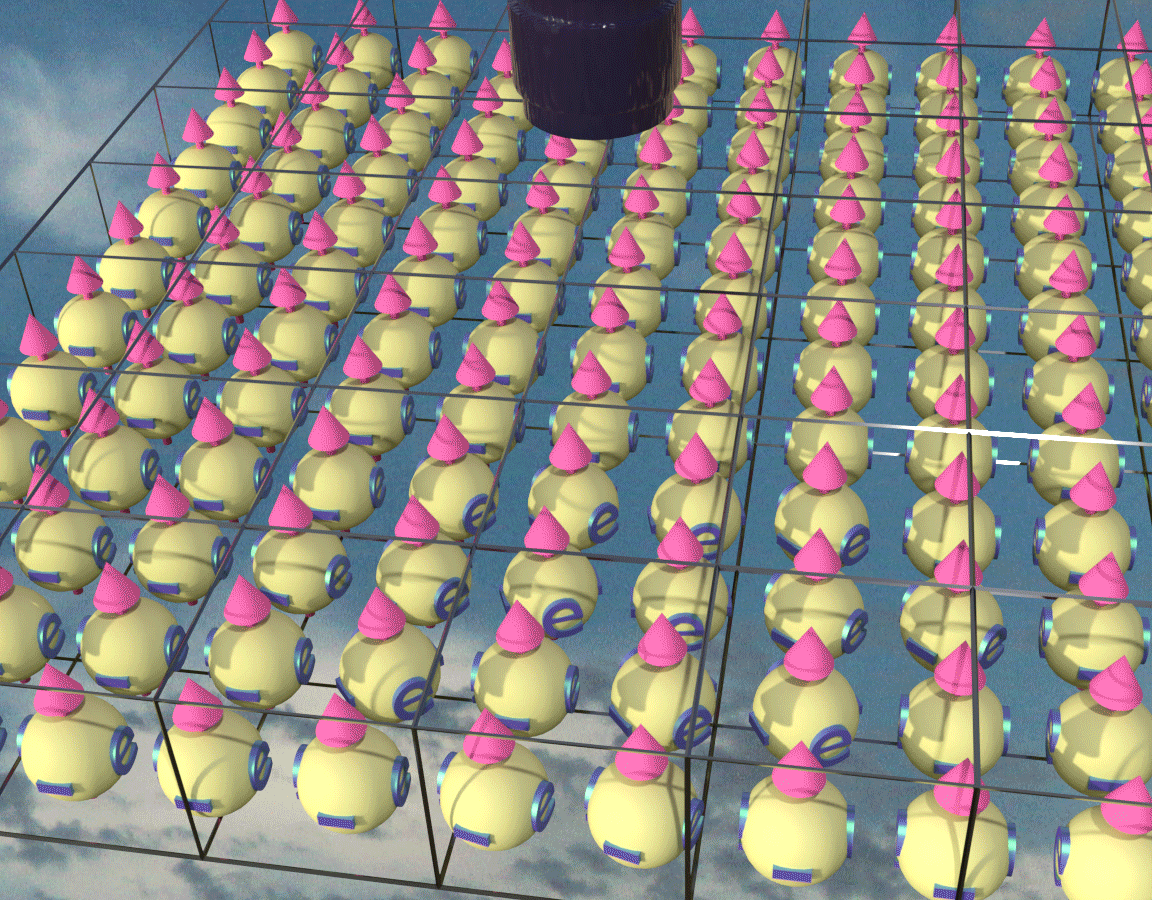
A high-speed optical memory consists of a high-speed demultiplexer and several memory cells. The task of the demultiplexer is to send each pulse of the train of many data pulses into an individual memory cell ensuring that other pulses have no effect on that cell.
 |
Fig. Operational principal of high-speed memory. The speed of the memory is determined by speed of demultiplexer |
The required operational speeds of the demultiplexer and the memory cell are very different. The demultiplexer should be very fast and be able to switch pulses within the time interval between two neighbor pulses, which is 1 picosecond in this example.
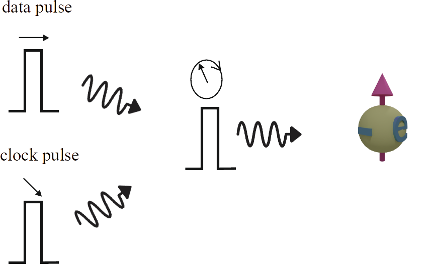
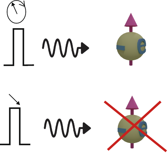
(main idea): A circular-polarized optical pulse excites spin-polarized electrons and, therefore, is recorded into the magnetic memory. In contrast, a linearly -polarized optical pulse does not excite spin-polarized electrons and, therefore, has no influence on the magnetic recording.
Two types of optical pulses are used in high-speed optical communication. The 1st type is data pulses and the 2nd type is clock pulse. The clock pulse is used for synchronization. It selects one one pulse from a train of data pulses for a recording.
The data and clock pulses are linear and cross polarized. When two pulses are combined, the resulting pulse is circular polarized, when the phase between pulses equals a quarter of wavelength.
| Selecting a data pulse for a recording | Demultiplexing principle | |
|---|---|---|
 |
 |
|
| A clock pulse is used for a selection. The data and clock pulse are linear and cross polarized. When two pulses are combined, the resulting pulse is circular polarized, when the phase between pulses equals a quarter of wavelength. | A circular-polarized optical pulse excites spin-polarized electrons and, therefore, is recorded into the magnetic memory. In contrast, a linearly -polarized optical pulse does not excite spin-polarized electrons and, therefore, has no influence on the magnetic recording. |
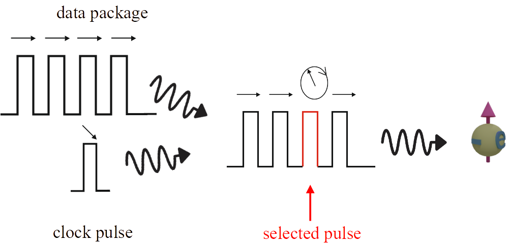
 How does demultiplexing work?
One specific data pulse can be selected from a train of data pulses by using a different delay of the clock pulse.
When a data pulse is selected, it becomes circular- polarized. As a result, only 0 or 1 data encoded in this pulse is recorded into the memory cell. Other data pulses remain linearly polarized and, therefore, have no influence on the recording.
| Selection of 2nd pulse for recording | Selection of 3d pulse for recording | |
|---|---|---|
 |
 |
|
| at this delay only the 2nd pulse is circularly polarized. As a result, data encoded in this pulse is recorded into the memory cell. Other data pulses remain linearly polarized and, therefore, have no influence on the recording. | at this delay only the 3rd pulse is circularly polarized. As a result, data encoded in this pulse is recorded into the memory cell. Other data pulses remain linearly polarized and, therefore, have no influence on the recording. |
| Demultiplexing scheme for multi cell memory. |
|---|
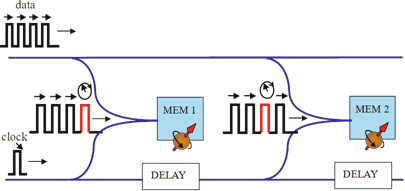 |
the demultiplexing scheme for multi cell memory:
There are two inputs for the data and clock pulses.
At the 1st memory cell the clock and data pulses combine so that the 1st data pulse becomes circularly polarized and, therefore, the data of only the 1st pulse is recorded into the into the memory cell number one
There is a delay for the clock pulse, so that at the 2nd memory cell the 2nd data becomes circularly polarized and, therefore, the data of only the 2nd pulse is recorded into the memory cell number two and so on.
It was measured experimentally that this demultiplexing scheme is able to do the demultiplexing for the train of the data pulses with the period as short as 100 femtoseconds (See below)
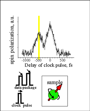
 Experimental verification of ultra- high speed of photon- to spin demultiplexing
 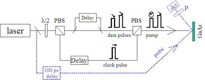 |
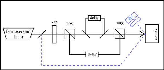 |
 |
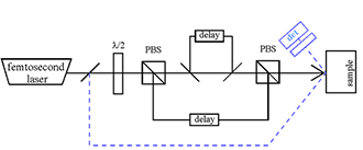
Experimental setup. The train of two data pulses combines with a clock pulse and is focused into a GaAs sample exciting the spin polarization. The amount of the spin polarization is measured from the Kerr rotation of the probe pulse, which is focused into the same spot. |
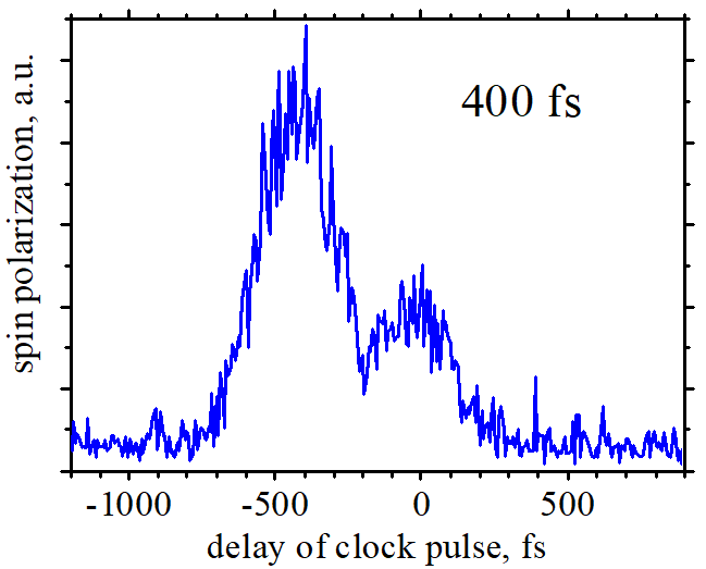
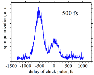
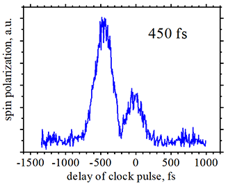
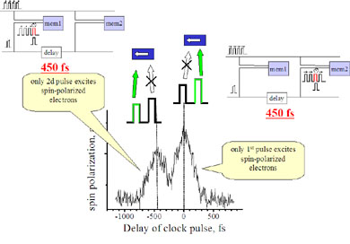
Fig.4 Pulse propagation | Measured spin polarization of photo-excited electrons in GaAs at T=70 K as a function of the delay between the clock pulse and train of two data pulses. Interval between data pulses 450 fs; |
| Verification of ultra- high speed of Photon- to- spin demultiplexing | |||||
|---|---|---|---|---|---|
|
|||||
| Spin polarization measured at a different delay between a train of two data pulses and a clock pulse. As the timing of the clock pulse coincide with one of the data pulses, the spin polarization is excited. | |||||
| Interval between two data pulses: 400 ps (left graph); 450 fs (central graph); 500 fs (right graph) | |||||
| For a delay of 450 fs and longer, each data pulse is clearly distinguished, meaning that only one data pulse creates spin polarization without any influence of the 2nd pulse. As a result, one data pulse can be demultiplexed from a train of many data pulses, even though the interval between pulses is extremely short (450 femtoseconds). | |||||
In order to verify the speed of the proposed multiplexing scheme, we use GaAs as a photon- to- spin converter and measure the spin-polarization excited by a train of two data pulses and a clock pulse. Figure above shows the spin-polarization as a function of a delay of the clock with respect to data pulses measured for a different period of the data pulses. For the period of 450 fs and longer each data pulse is clearly distinguished meaning that the clock pulse is able to select each individual pulse from a train of a short pulses with repetition rate of 2.2 TBit/sec.
 |
 |
|
|||||
Fig.6 Spin polarization of electrons excited by combined beam of clock pulse and two data pulse as a function of delay of clock pulse. For each point, the delay length was (n+1/4)lambda, where n is integer. Reading of spin polarization was done 100 ps after arrival of pump pulses |
Fig.7 Kerr rotation of probe pulse as a function of delay between clock and a single data pulses. The data proves a feasibility for recording at 2.2 TBit/sec. Insets shows that even with this speed one pulse will be memorized per each memory cell | Setup was used to verify multiplexing speed of spin-photon memory of 2.2 TBit/sec. |

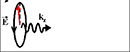
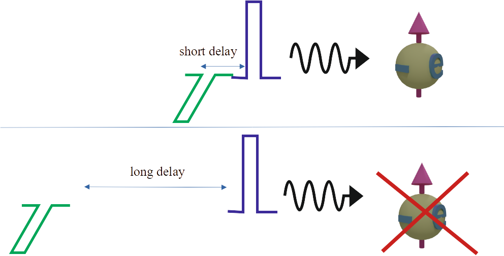
| Two consequent linear cross- polarized pulses can excite the spin, when the delay between pulses is short |
|---|
 |
| click on image to enlarge it |
You may wonder why there is a speed limitation for this demultiplexing scheme. It should be infinitely fast, because its operational principle is simple and straightforward. A circularly- polarized optical pulse excites the spin and a linearly- polarized optical pulse does not excite the spin. The event output is just "yes" or "no", there is nothing between.
It is not entirely true. In this example, the delay between two linear cross- polarized pulses equals, for example, is 50 femtoseconds and the combination of these two pulses excite the spin. It is an experimental fact. You can see that in this case the light is only linearly polarized and there is no circular polarization at any moment of time. Still these pulses excite the spin.
(experimental fact): Two consequent linear cross- polarized pulses excite the spin, even though there a delay between pulses and there is no circular polarized light at any moment of time
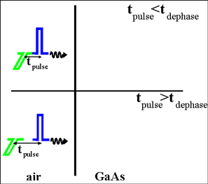
This unwanted effect (the electron dephasing time) is slowing down the demultiplexing speed of the photon- to- spin conversion.
 (a good fact): Since the electron dephasing time is very short (less than 100 femtoseconds), it only limits demultiplexing speed when the transfer rate approaches 10 Tbit/sec.
| Creation of the spin by two consequent linear cross- polarized pulses | ||||
|---|---|---|---|---|
|
||||
| click on image to enlarge it |
(explanation of the effect):![]()
This effect occurs due to a coherent interaction of photo-excited electrons.
In fact, each linear-polarized pulse excites both spin-up and spin-down electrons in the equal amount.. Since the amount is equal, within a short time, the electrons are mixed up with other electrons and in total there is no spin transform into electron gas.
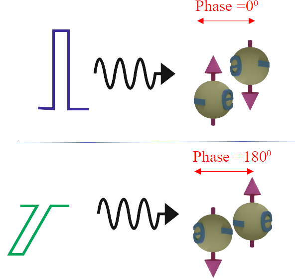
The phase between the wave function of photo-excited spin-up and spin-down electrons is fixed. A Pulse of a different direction of the linear polarization produces a pair of the spin-up and spin-down electrons of a different phase between them. For example, the phase difference is 0 deg for this direction of light polarization and180 deg for this polarization
The remaining spin polarization, which is excited by two consequent optical pulses, depends on the delay between pulses. When the delay is long, the spin-up and spin-down electrons, which are excited by each pulse, are dissolved within other electrons of the electron gas and there is no spin transfer.
When the delay is short, the spin-up and spin-down electrons, which are excited by each pulse, interact coherently according to their phase resulting in the spin transform from optical pulses to the electron gas.
Figure 33 (on the right) demonstrates this effect. In the case of a short delay between optical pulses, the spin-up and spin-down photo-excited electrons remain in their mutual phase and , therefore, interact coherently, which finally results in a remaining non-zero spin polarization. In contrast, in the case of a long delay between optical pulses, the spin-up and spin-down photo-excited electrons lose their mutual phase before the 2nd pulse arrives. There is no coherent interaction and no remaining spin polarization.
![]() The electron dephasing time is the period of time, after which the electron loses its initial phase due to interaction with other conduction electrons or other objects. It is the time within which a conduction electron interacts with its own environment.
The electron dephasing time is the period of time, after which the electron loses its initial phase due to interaction with other conduction electrons or other objects. It is the time within which a conduction electron interacts with its own environment.
![]() I believe electron dephasing time is one of shortest relaxation times in a solid
I believe electron dephasing time is one of shortest relaxation times in a solid
I have measured the dephasing time in GaAs. It equals 450 femtoseconds at a temperature of 70 K (see above) . The dephasing time is even shorter at room temperature.
![]() Why the dephasing time is short and why does it influence the spin?
Why the dephasing time is short and why does it influence the spin?
The dephasing time is very short, because it is just time until the photo excited electrons interact with many of their neighbor electrons in the electron gas. Generally, such an interaction is individual for each electron. Therefore,the interaction of either spin-up or spin-down electrons with neighbors leads to a loss of their mutual phase.
![]() (fact): In many materials, the efficiency of photon-to-electron spin transfer is poor.
(fact): In many materials, the efficiency of photon-to-electron spin transfer is poor.
Additionally to the spin, a conduction electron may have an orbital moment. and the spin of a photon can be transformed either into the electron spin or into the orbital moment or partly into both of them. There are two distinguished paths for the spin of a photon to be absorbed by a solid:
![]() (path 1) the spin of a photon is transformed into the spin of electrons and does not affect the orbital moment. In this case, the spins of all photo-excited electrons are directed in one direction along the spin of the photon and, therefore, the photo-excited electrons become spin-polarized and enable to reverse the magnetization.
(path 1) the spin of a photon is transformed into the spin of electrons and does not affect the orbital moment. In this case, the spins of all photo-excited electrons are directed in one direction along the spin of the photon and, therefore, the photo-excited electrons become spin-polarized and enable to reverse the magnetization.
![]() (path 2) the spin of a photon is transformed to the orbital moment and does not affect the spin of electrons. As a result, the spin polarization of the photo-excited electrons remains exactly the same as the spin polarization of the conduction electrons in the equilibrium, which means that the optical pulse has no effect on the spin polarization of the electron gas and, therefore, on the magnetization.
(path 2) the spin of a photon is transformed to the orbital moment and does not affect the spin of electrons. As a result, the spin polarization of the photo-excited electrons remains exactly the same as the spin polarization of the conduction electrons in the equilibrium, which means that the optical pulse has no effect on the spin polarization of the electron gas and, therefore, on the magnetization.
For example, when the orbital state is zero L=0 and the excited state is one L=1, the spin of a photon is absorbed into the orbital moment and the photo-excited electrons are not spin- polarized.
In order for the all-optical magnetization to become effective, the optical transitions of the 1st type should be enhanced and the transitions of the 2nd type should be suppressed.![]() When a linear polarized light is absorbed by a material having different orbital moment for the ground and excited states, where is the spin to supply for the orbital moment change?
When a linear polarized light is absorbed by a material having different orbital moment for the ground and excited states, where is the spin to supply for the orbital moment change?
An excited-electron state with L=+1 has an identical electron state with L=-1, because of the conversion of the time- inverse- symmetry. A linearly- polarized light can be decomposed into a sum of left- and right- circular- polarized light. Therefore, the photons have two opposite spins. One spin is transferred to the band L=+1 and another spin is transferred to the band L=-1.
( How to increase efficiency of the Photon- to- Spin Conversion): Make a "magical material, in which the orbital moment for all optically-excited states is the same as for the ground state.
All possible optical transitions in the "magical" material should not be affected by the orbital moment.
![]() In this case, the spin of photons is transformed into the spin of the conduction electrons, increasing the number of the spin-polarized electrons. It means that the difference between the orbital moment of the ground electron state and the optically-excited electron state should be as small as possible. Ideally, the orbital moment should be the same for both states.
In this case, the spin of photons is transformed into the spin of the conduction electrons, increasing the number of the spin-polarized electrons. It means that the difference between the orbital moment of the ground electron state and the optically-excited electron state should be as small as possible. Ideally, the orbital moment should be the same for both states.
This property is rare in a material, but it can be designed or engineered.
How to make the same orbital moment for the ground state nor the excited state.
(method 1) Quench of the orbital moment.
When the orbital moment is quenched (See here) , neither ground state nor excited state have any orbital moment.
(method 2) Intraband transitions
Additional possibility is to make a material, in which the ground and excited states belong to the same band. That means that the ground and excited states for an optical transition have the same orbital moment and the spin of a photon is fully transformed into the spin of the electron. Such optical transition is called the Intraband transition and has been used in quantum- cascade lasers. This technology is well- known and is already commercialized.
In general, the orbital moment of the conduction and valence electrons is not quenched and there is a large difference between the orbital moment for ground and excited states. As a result, a little of the photon spin is transformed into the spin of the electron making the all-optical switching ineffective.
Methods to quench the orbital moment of the conduction and valence electrons in a solid:
(method 1) Electron confinement (Quantum wells, quantum dots and surface states)
All these types of electron confinement make a conduction electron similar to a localized electron and, as a result, quenching its orbital moment
![]() (fact) The orbital moment of localized electrons is nearly- fully quenched (See here)
(fact) The orbital moment of localized electrons is nearly- fully quenched (See here)
As a result, the localized electrons are ideal for an efficient photon- to- spin conversion. Unfortunately, the light only weakly interact with the localized electrons (see above)
![]() (fact) the light is absorbed by the conduction electrons, but not by the localized electrons (See above).
(fact) the light is absorbed by the conduction electrons, but not by the localized electrons (See above).
As a result, the spin of a photon is transformed to the spin of the conduction electrons at first. Next, the spin of the conduction electrons is transformed to the spin of the localized electrons.
![]() (fact) A conduction electron and a localized electron interact most efficiently, when they have a similar spatial symmetry.
(fact) A conduction electron and a localized electron interact most efficiently, when they have a similar spatial symmetry.
![]()
![]()
![]() When a conduction electron and a localized electron have a similar spatial symmetry, the spin transfer from conduction electrons to the localized electrons is the most efficient.
When a conduction electron and a localized electron have a similar spatial symmetry, the spin transfer from conduction electrons to the localized electrons is the most efficient.
For example, in the case of the toggle switching (see above), the heating of the d- and f- electrons is different, because of a different efficiency of the interaction of the conduction electrons with localized electrons of the d- and f- symmetry.
The best spatial symmetry of efficient spin conversion:
(localized electrons): d- symmetry
(conduction electrons): p- symmetry (with some d-symmetry component)
![]() Usually, it is difficult to satisfy these conditions in the bulk of a material, but it is possible at an interface between two materials
Usually, it is difficult to satisfy these conditions in the bulk of a material, but it is possible at an interface between two materials
(choice 1): ferromagnetic material
In this case, both functions the photon- to- spin conversion and the memory function are in one ferromagnetic material
(choice 2): non-magnetic material
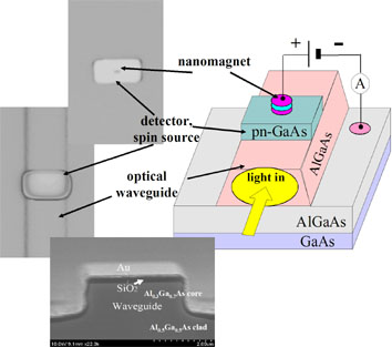 |
Fabricated spin-photon memory. As a photon-to- spin converter, a pn- GaAs photodetector is used. As a memory cell, a Fe nanomagnet is used. The circular- polarized light is absorbed in a pn- GaAs photodetector. The photo-excited spin- polarized electrons are injected to the nanomagnet to reverse the magnetization |
In this case, both functions the photon- to- spin conversion and the memory function are in one ferromagnetic material
To find or to design or to engineer a material with a high conversion efficiency from the Spin of a Photon to the Spin of an Electron is difficult. It is even more difficult to find such a material only among ferromagnetic materials. A ferromagnetic material is required for storage of data.
It is not necessary that both functions are realized in a single material. An efficient spin-conversion may be done in a non-magnetic material and then spin- polarized electrons are injected into a ferromagnetic material for a recording. A possibility to find the "magical material" for the spin conversion is higher if the search is extended among non-magnetic materials.
For example, I have fabricated and studied the spin-photon memory, in which a semiconductor is used as a spin-converted. The photo-excited spin-polarized electrons are injected in ferromagnetic nanomagnet for a recording. The optical transition is simpler and, therefore, it is easier to optimize the semiconductor for an efficient spin conversion (see here)
 |
|---|
Intermag 2023. |
|---|
 |
| click to see Youtube Video |
I will try to answer your questions as soon as possible