Dr. Vadym Zayets
v.zayets(at)gmail.com
My Research and Inventions
click here to see all content |

Dr. Vadym Zayetsv.zayets(at)gmail.com |
|
|
Spin -Photon memory
High-speed demultiplexing experimentIn this experiment it was proved that recording speed of the spin-photon memory can reach 2.2 TBit/sec. In the design of the spin-photon memory, data pulses excite the spin-polarized electrons and afterwards this spin information is memorized. The memory speed is the fastest when a data package with shortest interval between pulses still could be memorized. The interval between pulses is shortest when it is still possible to excite the spin only by one pulse in the package of many pulses without any influence of other pulses. We have experimentally proved that for a package with pulse interval of 450 fs it possible to excite the spin only by one pulse without influence of other pulses.
|
| Part 1. Dimulteplexing |
|---|
|
 |
Fig.1 Operational principal of high-speed memory. The speed of the memory is determined by speed of demultiplexer |
The operation of any high-speed memory or buffer memory is different from the operation of random access memory (RAM). The buffer memory operates with packages of data pulses rather than with a single pulse. The interval between pulses in a package is very short ( few picoseconds(ps) or less), but interval between recording or reading of packages is relative long (about 100 picoseconds-1 nanosecond).
The closer the pulses can be placed relatively to each other, the more data can be transferred through one line and the faster recording speed of memory can be achieved. The minimum interval between pulses, at which a pulse can be recorded without any influence of nearest pulse, determines the recording speed of the memory.
Any high-speed memory consists of two essential parts: a high-speed demultiplexer and a storing media. The high-speed demultiplexer redistributes the train of data pulses into an individual memory cells ensuring that only one pulse is memorized per each memory cell. The memory cell is storing the data. The recording speed of the memory is limited only by the speed of the demultiplexer. The spin-photon memory combines both the high-speed optical demultiplexing and the non-volatile data storage.
It is important to emphasize that two functions of high-speed memory may have very different timing. If the demultiplexing should be very fast, the memorization could take longer time. For example, in the case when the interval between pulses in packages is 1 ps and the interval between packages is 1 ns, the switching time of the demultiplexer (spin switching in our case) should be less than 1 ps, but magnetization reversal could take longer time up to 1 ns. For example, 100 ps for magnetization reversal is sufficiently short time.
 |
Fig.2 Maximum speed of memory. Pulse interval is shortest, but only one pulse is memorized per one memory |
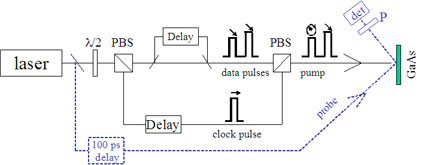
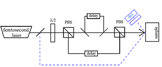
Figure 3 shows the experimental setup. A mode-locked Ti:sapphire laser (lambda=820 nm ) provides 160 fs linearly-polarized pump and probe pulses. Polarization of the pump was rotated by a lambda/2 waveplate and split by polarization beam splitter (PBS) into clock pulse and data pulse of linear and mutually orthogonal polarizations. The data pulse was split into two pulses. The second data pulse was 165 lambda (~450 fs) delayed. Clock and data pulses were combined together by another PBS and focused on the sample. The linearly polarized probe beam was 100 ps delayed relatively to the pump and focused on the same spot on the sample. The spin polarization of electrons excited by pump beam was estimated from Kerr rotation angle of the probe beam.
 |
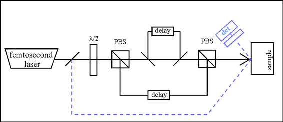 |
Fig.3 Experimental setup |
Fig.4 Pulse propagation |
The rotation angle of reflected probe beam was measuring by polarizer (P) and photo detector (det). Intensity of each data pulse was 1-10 microJ/cm2. Intensity of the probe pulse was 10 times smaller. The data pulses and clock pulse were phase locked. When the clock pulse and one of data pulse nearly coincided, the positive and negative angles of Kerr rotation were observed for delays of (n+1/4)lambda and (n-1/4)lambda, respectively (See Fig.5). When the pulses were away from each other, the Kerr rotation was not observed.
 |
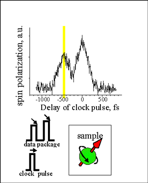
Fig.5 Kerr rotation of probe pulse as a function of delay between clock and a single data pulses |
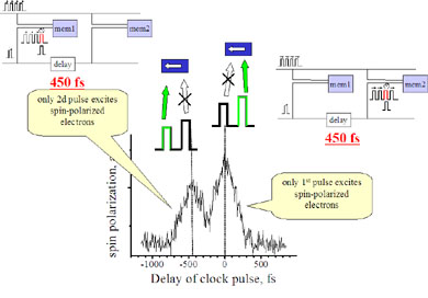
Figure 6 shows spin polarization of the excited electrons by a single clock pulse and two data pulses (interval between data pulses is 450 femtoseconds) as a function of delay between clock pulse and first data pulse. It is major result of this experiment. For each point the delay length was equal to (n+1/4)l, where n is an integer. The maximum of spin polarization was observed when the clock pulse coincides with first data pulse. The spin polarization decreases when the clock pulse is delayed out of the first data pulse, and again increases as the clock pulse coincides with the second data pulse. Fig. 6 clearly shows that the spin polarization excited by the second data pulse can be separately distinguishable from the spin polarization excited by the first data pulse. This means that from two closely placed optical data pulses, only one pulse can trigger the recording without influence of another pulse. The interval between the data pulses is 450 fs. It corresponds to the recording speed of 2.2 TBit/sec. Notice that the detection of spin polarization was done 100 ps after data pulse arrived. This means that the lifetime of the spin polarized electrons is sufficient long to inject the spin polarized electrons into the nanomagnet for the magnetization reversal.
For the memory operating at speed 2.2 TBit/sec, the delay of clock pulse between cells (Fig. 7) should be (~450 fs), the initial magnetization of all nanomagnets should be spin down and the delay of data pulses relatively to the clock pulse should be (1/4+m*165) lambda, where m is a number of the data pulse. As result of Fig. 7, in this case in each cell only one data pulse excites spin polarization and memorized there. Other data pulses have no influence on spin polarization of that cell. In our experiment, the shortest interval between the data pulses, when the spin polarization excited by each pulse can be individually distinguished, is about 450 fs. For shorter interval the spin polarization is overlapped and the spin polarization created by preceding data pulse is reduced by next data pulse, which is causing overwriting of data of preceding pulse by next pulse in the cell. Therefore, the memory can not operate at speed faster than 2.2 TBit/sec.
 |
 |
|
Fig.6 Spin polarization of electrons excited by combined beam of clock pulse and two data pulse as a function of delay of clock pulse. For each point, the delay length was (n+1/4)lambda, where n is integer. Reading of spin polarization was done 100 ps after arrival of pump pulses |
_____ | Fig.7 Kerr rotation of probe pulse as a function of delay between clock and a single data pulses. The data proves a feasibility for recording at 2.2 TBit/sec. Insets shows that even with this speed one pulse will be memorized per each memory cell |
To reach the operation speed of a memory above 1 TBit/sec, the physical mechanisms responsible for recording should have relaxation time shorter than 1 ps.
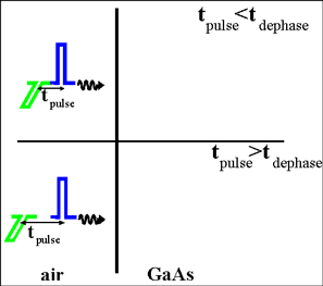 |
Fig.8 Excitation of spin-poalarized electrons by two linearly cross-polarized optical pulses. a) interval between pulses is shorter than electron dephasing time. Excited electron are spin-polarized. b) interval between pulses is longer than electron dephasing time. Excited electron are not spin-polarized |
It is impossible to make a demultiplexer with infinite operational speed. The nature always put some limitations. It is important that a relaxation time, which limits the switching speed of the demultiplexer should be as short as possible. In the case of spin-photon memory the time, which limits the switching, is electron dephasing time. It is very short. At least, it is shorter than 500 fs.
Figure 8 explains how the electron dephasing time limits the switching speed of the spin-photon memory. In the design of the spin-photon memory two linearly cross-polarized pulses combine into circularly-polarized pulse and excite a spin. When there is some interval between pulses the spin should not be excited. However, spin-polarized electrons can be excited by two linearly cross-polarized pulses even the pulses arrived at different time. If the dephasing time is longer than the interval between pulses, the electrons excited by two pulses can coherently interfere and create spin polarization.
Phase-locked pump-probe experiment |
 |
|
| Setup was used to verify multiplexing speed of spin-photon memory of 2.2 TBit/sec. |
I will try to answer your questions as soon as possible

 Video
Video 
