Dr. Vadym Zayets
v.zayets(at)gmail.com
My Research and Inventions
click here to see all content |

Dr. Vadym Zayetsv.zayets(at)gmail.com |
|
|
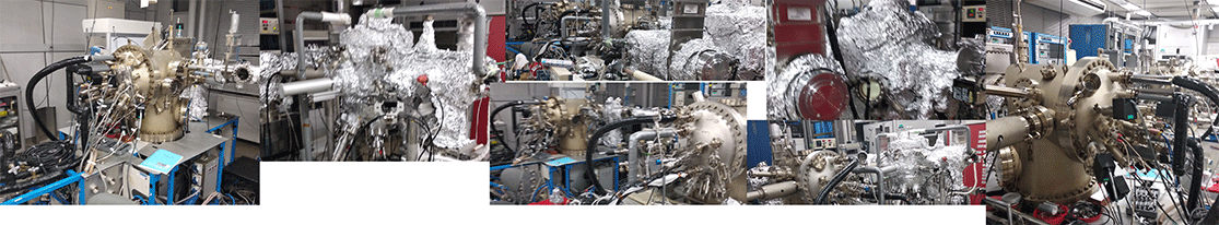
Technologiesdeveloped by Vadym Zayets in AIST (Tsukuba, Japan) from 1995 to 2018
Technology 1:
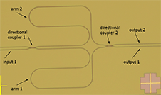
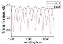
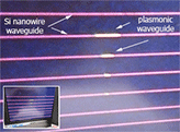
Fabrication of Si nanowire waveguide, including integrated polarizer, ring resonator and MZ interferometer.developed from 2012 till 2015Minimum dimension: 100 nm
Details see here and here
Technology 2:
Fabrication of a metallic nanowire with periodically modulated perpendicular magnetic anisotropy (a nanowire with periodical-stripe gate for all-metal transistor)developed from 2016nanowire width: 100nm;
Details see here
Technology 3:
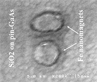
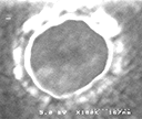
Fabrication of nanomagnet on top of semiconductor p-i-n photo detector with an Ohmic contact.developed from 2005 till 2010Minimum diameter: 100 nm Minimum gap: 40 nm
Details see here
Technology 4:
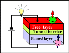
Fabrication of nanomagnet, nano-sized tunneling magnetic junction (MTJ)developed from 2010Minimum diameter: 50 nm Fabrication method: slimming
Technology 5:
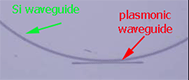
Fabrication of low-optical-loss plasmonic waveguidesdeveloped from 2008Minimum dimension: 50nm propagation loss: 0.7 dB/um (Fe,Co); 0.09 dB/um (Au);
Details see here
Technology 6:
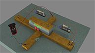
Measurement method for voltage-controlled magnetism in a ferromagnetic nanowiredeveloped from 2018Measurement precision:
Details see hereTechnology 7:
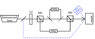
Setup of phase-locked pump-probe experimentdeveloped from 2005 till 2008Pump-probe delay precision: λ/90 Precision of switching speed measurement: 50 fs
Details see here
Technology 8:
Fiber-to-waveguide coupling setupdeveloped from 2000 till 2002A magnetic field up to 5 kGauss can be applied along or perpendicular to the waveguide. Alignment precision: 10 nm Alignment method: automatic
Details see hereTechnology 9:
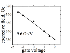
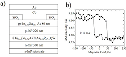
High-precision measurements of coercive and anisotropic fields, retention time, energy of magnetic anisotropy and Δdeveloped from 2017Max magnetic field: 7.2 kG out-plane and 2 kG in-plane. Measurement Precision: Coercive field: 0.1-0.9 Oe Anisotropic field: 10 Oe Unique features: 1. Magnetic field can be applied in any direction 2. High- precision measurements of coercive field
Details see hereTechnology 10:
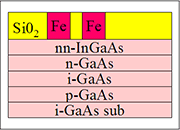
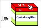
Fabricating and testing semiconductor optical amplifier (SOA), semiconductor laser diode (LED) and hybrid amplifierdeveloped from 1999 till 2005active region: MQW GaAsP/AlGaAs tensile-strained multi QW growth method: MBE
Details see hereTechnology 11:
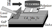
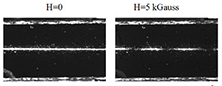
Optical isolator made of a diluted magnetic semiconductordeveloped from 1995 till 2005Magneto-optical material: CdMnTe grown on GaAs Coupling method: prism Propagation loss: 0.1 dB/mm Mode conversion ratio: 98% Isolation: 25 dB
Details see here
|
I will try to answer your questions as soon as possible