Dr. Vadym Zayets
v.zayets(at)gmail.com
My Research and Inventions
click here to see all content |

Dr. Vadym Zayetsv.zayets(at)gmail.com |
|
|
Spin -Photon memory
ReadingA reading function is essential for any memory. In the case of high-speed optical read-out of the spin photon memory the output is a package of optical pulses and the intensity of each pulse in the package is proportional to the magnetization direction of each memory cell. A main challenge to realize the reading function is to achieve reasonable signal-to-noise ratio (SNR) for reading of the magnetization of a nanomagnet, which has very small volume.
|
| Part 2. Reading function |
|---|
|
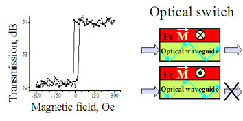 |
Fig.1 Read-out scheme utilizing the effect of the magnetization-dependent optical loss. The transmission through a hybrid waveguide can be switched on or off by reversing the magnetization of the ferromagnetic metal |
The magneto-optical read-out can be achieved by utilizing effect of magnetization-dependent loss. When one layer of the optical waveguide is ferromagnetic metal and its magnetization is perpendicular to the mode propagation direction, the optical absorption is different for two opposite direction of the magnetization. Therefore, such waveguide can function as an optical gate, when the light can be switched on or off by reversing the magnetization of the metal. The magnetization of a ferromagnetic metal can be detected by the intensity of transmitted light.
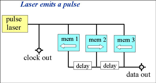 |
Fig.2 Multiplexing scheme for high-speed reading |
Figure 2 shows the multiplexing scheme for this memory. For each memory cell, the optical waveguide passes under the nanomagnet. Due to the effect of magnetization-dependent loss, the absorption of light in waveguide will be different for two opposite magnetization directions of the nanomagnet. The mode-locked laser, which could be integrated on the chip, provides the short pulses. The waveguide path is split, so that a laser pulse is split and it illuminates every memory cell. At output, all waveguide paths are combined. Each path has different length, so that each pulse reaches the output with a different delay and the amplitude of the pulse corresponded to the magnetization of each cell. Therefore, at the output the serial train of pulses will form with intensities proportional to the data stored in each memory cell. The speed of the reading is only limited by pulse width provided by the laser and it can be very fast.
 |
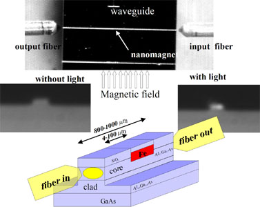 |
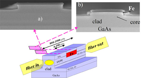
Fig.3 Measurements of magnetization-dependent loss in AlGaAs waveguide with embedded Fe nanomagnet. Cross-sectional SEM images shows the waveguide and waveguide with nanomagnet. |
Fig.4 Experimental setup to measure the magnetization dependent loss in waveguide with nanomagnet. Optical images of waveguide cross-section shows that the light propagate only inside waveguide |
(Al,Ga)As optical waveguide was grown by MBE. Following 3-mm-thick Al0.5Ga0.5As clad layer, the 800-nm-thick Al0.3 Ga0.7 As core layer was grown. The 120-nm-deep pit was wet etched through photo resist mask following the deposition of 40 nm of Fe and 5 nm of Au by sputtering. The metal was lift-off. Therefore, the metal remained only inside the pit. The rib waveguide was dry etched with a SiO2 mask. The height of the rib was 600 nm. The width of the rib and the Fe micromagnet were the same. The waveguide was covered by 200-nm-thick SiO2 to avoid oxidation. The devices with a variety of lengths of Fe nanomagnet were fabricated on the same wafer. The light of the wavelength of 770 nm was coupled in and out of the waveguide using polarization-maintaining fibers. The light intensity was 50-300 mW. The magnetic field was applied perpendicularly to the waveguide and in the film plane. Figure 3 shows the structure of the fabricated device. Figure 3(a) shows a scanning-electron-microscope (SEM) cross-section image of the waveguide taken across the waveguide and Fig. 3(b) shows SEM image taken across the nanomagnet. In both cases, the waveguide walls were vertical and the interface between semiconductor and Fe nanomagnet was smooth.
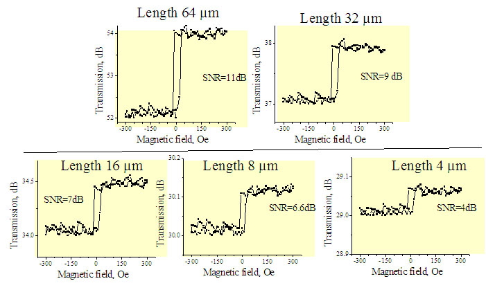 |
Fig.5 Transmission of waveguiding light as function of the magnetic field for different lengths of nanomagnet |
Figure 5 shows the transmission coefficient of TM waveguide mode as a function of the applied magnetic field for the 3-mm-wide waveguide with the micromagnet length of 64 um, 32 um,16 um, 8 um and 4 um. Clear hysteresis loop for the transmission coefficient was observed in all cases, but amplitude of the loop was smaller in the case of the shorter micromagnet. The loop was not observed in the case of a waveguide without Fe micromagnet. It proves that the transmission depends on the magnetization direction of the Fe micromagnet. With decreasing of the micromagnet length, both the magneto-optical (MO) signal and signal-to-noise ratio (SNR) decrease.
Figure 6 shows the fiber-to fiber loss, MO signal and SNR as a function of the length of the Fe micromagnet. The loss is linearly proportional to the length of Fe micromagnet as 0.38 dB/um. The offset loss of 27 dB is due to the fiber-waveguide coupling loss and the scattering loss on Fe micromagnet. MO signal is linearly proportional to the micromagnet length for lengths longer than 10 mm. For shorter lengths, the MO signal rapidly decreases. Therefore, in the case when the micromagnet size is comparable with the wavelength, the linear proportionality of MO signal to the Fe micromagnet length does not hold. The SNR is almost constant around 10 dB for the long lengths, but it rapidly decreases when the micromagnet length becomes comparable with the wavelength of light (lambda=770 nm).
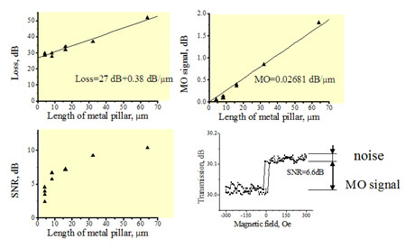 |
Fig.6 Fiber-to-fiber optical loss, magnetization-dependent optical loss and signal-to-noise ratio of in AlGaAs waveguide with embedded Fe nanomagnet as a function of nanomagnet length. |
From Fig. 5 it clear that to get sufficient readout signal the size of nanomagnet should be few micrometers or larger. However, for the recording the size of nanomagnet should be as small as possible. At least it should be smaller than 100 x 100 nm. To resolve this trade-off we proposed the readout scheme, which utilizes the spin injection.
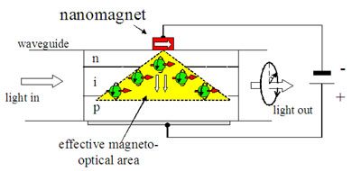 |
Fig.5 Proposed design for detection of the magnetization utilizing the spin injection from the nanomagnet into p-i-n junction |
In the most desirable case, the read-out efficiency should not depend on the size of the micromagnet. Therefore, the sizes of the micromagnet could be optimized according to the conditions for the recording. Figure 4 shows a scheme for the proposed solution, which satisfied this condition. The device consists of a nanomagnet fabricated on top of a p-i-n junction. The device structure is the same as it was used for recording , except the polarity of the applied voltage between micromagnet and p-region is reversed. In the case of recording, the spin-polarized electrons are injected from the p-i-n junction into the nanomagnet. In the proposed scheme for read-out, the spin-polarized electrons are injected from the nanomagnet into the p-i-n junction. The input optical pulse of wavelength corresponded to the bandgap of the i-region is used for the read-out. Under forward electrical bias the spin-polarized electrons and unpolarized holes are injected into the i-region of the p-i-n junction and recombines there with the result of stimulated emission and amplification of the input pulse. Due to the optical selection rule, the amplification for the left and right circular polarizations is different when electrons in amplifying region are spin-polarized. The polarization of linearly polarized light will be rotated in this p-i-n junction. The direction of rotation will correspond to the direction of the nanomagnet magnetization. Therefore, by detecting the direction of polarization rotation of output pulse, the data stored in the memory can be read. Due to wide spreading of spin-polarized electrons over a larger volume in the p-i-n junction, the effective volume of magneto-optical area will be significantly larger than the volume of nanomagnet. Assuming that the electron spreading has the shape of rotational semi-ellipsoid , the effective magneto-optical volume could be as large as 0.1 um^3, comparing with only 1E-4 um^3 of nanomagnet volume. Therefore, it could be expected that in this case the magneto-optical signal will be significantly greater. Moreover, due to optical gain, the magneto-optical signal could be further amplified.
I will try to answer your questions as soon as possible

 Video
Video 