Dr. Vadym Zayets
v.zayets(at)gmail.com
My Research and Inventions
click here to see all content |

Dr. Vadym Zayetsv.zayets(at)gmail.com |
|
|
Spin -Photon memory
Spin-photon memory with MTJ electrode
Major advantage of spin-photon memory with MTJ (magnetic tunnel junction) electrode is its ability for both electrical and optical reading and writing. Because of this property, major application of this memory is chip-to-chip connection. The reading and recording in the spin-photon memory with MTJ is easier to realize than in the case of spin-photon memory with nanomagnet. Major disadvantage of this memory is the limitation of number of optical pulses in a data package, which could be recorded.
|
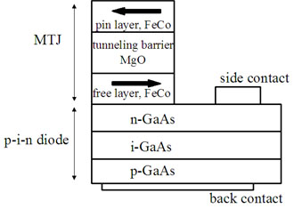 |
Fig.1 Design of spin-photon memory with MTJ electrode |
Figure 1 shows an example of spin-photon memory with MTJ electrode. It consists of GaAs p-i-n diode with magnetic tunnel junction (MTJ) electrode. The MTJ is made of two ferromagnetic metal region separated by non-conductive tunneling region (MgO layer in Fig.1). The ferromagnetic metal region, which contacted to the n-GaAs, is named free layer. Other ferromagnetic metal region is named pin layer. The current-induced torques required to change magnetization direction is smaller for the free layer than for the pin layer. The resistivity of MTJ depends on mutual orientation of magnetization of free and pin layers. Also, there is the non-magnetic side contact to n-GaAs and the non-magnetic back contact to p-GaAs.
The free layer has two stable magnetization directions. The data is stored as a magnetized direction in the free layer. The magnetization of pin-layer is not changed.
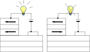 |
Fig.2 Electrical reading. When magnetization of free layer is parallel to magnetization of pin layer, the MTJ resistivity is low, when the magnetization is opposite, the resistivity is high. |
The methods of electrical recording and reading in the spin-photon memory with MTJ electrode is the similar to the recording and reading methods which are currently used in MRAM (magnetic random access memory).
For the electrical reading, a voltage is applied between the MTJ and the side contact. Since the resistivity of MTJ is smaller when the magnetization of free layer is parallel to the magnetization of the pin layer and the resistivity is larger when the magnetization of free layer is opposite to the magnetization of the pin layer. For the reading, the voltage is applied between the side electrode and the MTJ. The flowing current is different for two opposite magnetization directions of the free layer in respect to the magnetization direction of the pin layer. Therefore, the output current corresponds to data stored in the memory cell.
For the electrical recording, the larger voltage is applied between the MTJ and the side contact. The charge current generates a spin current at the tunnel barrier. The spin transfer torque is a consequence of the transfer of spin angular momentum from a spin current to the magnetic moment of the free layer. If the current is sufficient, the magnetization of the free layer is reversed. By changing polarity of the applied voltage, the magnetization of free layer can be turn either parallel or opposite to magnetization of the pin layer.
The method of high-speed optical recording method for this memory is the same as the recording method for spin-photon memory with nanomagnet. The circularly-polarized optical pulse is absorbed in the p-i-n GaAs creating spin-polarized electrons. Under voltage applied between MTJ and back electrode these spin polarized electrons are injected from the semiconductor into the free layer of MTJ. The spin transfer torque is a consequence of the transfer of spin angular momentum from a spin-polarized current to the magnetic moment of the free layer of MTJ. If the torque is sufficient, the magnetization turns and the data is memorized.
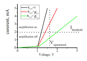 |
Fig.3 IV characteristic of p-i-n optical amplifier with MTJ electrode. The red line shows the case when the magnetization of free layer is parallel to the magnetization of pin layer. The green line shows the case when the magnetization of free layer is opposite to the magnetization of pin layer. The black line shows the case of a zero-resistance electrode |
However, in contrast to spin-photon memory with nanomagnet, in the case of the memory with MTJ, a linear-polarized pulse of sufficient intensity may reverse the magnetization of free layer. It is an undesirable event. In the scheme of high-speed demultiplexing, the recorded pulse has circular polarization. Other pulses in the optical package are linear polarized and should not have influence on the recording. Therefore, in the memory with MTJ the generation of spin current at the tunnel barrier should be minimized. The memory should be optimized so that the threshold current for magnetization reversal by spin-polarized current should be significantly smaller than the threshold for unpolarized current. In any case, the number of pulse in optical package used for recording in the spin-photon memory with MTJ electrode is limited.
The high-speed optical reading is easier to realize in the of the memory with than in the case of the memory with nanomagnet.
The voltage is applied between the MTJ electrode and the back contact. The polarity of the voltage is such so that the p-i-n junction is in direct bias. In the case when the current flowing through the p-i-n junction exceeds a threshold current, the p-i-n provides optical gain and the amplitude of optical pulse passing through the p-i-n junction increases.
 |
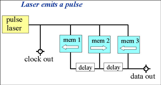 |
| Fig.4 Optical reading of magnetization of the free layer. | Fig.5 Multiplexing scheme for high-speed reading |
Figure 3 shows IV characteristic of a p-i-n junction with MTJ electrode, in which the magnetization of free layer is either parallel or opposite to the magnetization of the pin layer. The operational voltage is such that the optical amplifier provides optical gain in the case of the magnetization of free layer is parallel to the magnetization of the pin layer and the optical amplifier does not provide optical gain when the magnetizations are opposite.
Figure 5 shows the multiplexing scheme. The mode-locked laser, which could be integrated on the chip, provides the short pulses. The waveguide path is split, so that a pulse is split and it illuminates every memory cell. At output, all waveguide paths are combined. Each path has different length, so that each pulse reaches the output with a different delay and the amplitude of the pulse corresponded to the magnetization of each cell. Therefore, at the output the serial train of pulses will form with intensities proportional to the data stored in each memory cell. The speed of the reading is limited only by a shortest pulse width, for each the p-i-n junction is able to provide an optical gain.
 |
Fig.6 Resistance-area product of Fe:MgO:Fe MTJ as a function of MgO thickness |
The fabrication of the MTJ with very thin tunnel barrier and very thin free layer on top of the semiconductor is main challenge of the fabrication. The following estimations explain the important of a thin tunnel barrier, a thin free layer and low semiconductor/metal contact resistance for the fabrication of spin-photon memory with MTJ.
From MRAM technology it is known that there is a threshold current, above which current-induced magnetization reversal is possible. The threshold current is proportional to the volume of the free layer. Typically the threshold current density is 1E7 A cm2= 100 mA um2. Therefore, in order to reverse magnetization of the free layer with area of 100 nm x 100 nm, typically the current of 1 mA is required. In commercial MRAM the size of area of free layer is much smaller. As far as I know, in the commercial MRAM the threshold current for the magnetization reversal is about 0.05 mA. (It so easy to generate such current even with a very weak optical pulse!).
The maximum voltage, which may be applied to MTJ is about 1-10 V. The higher voltage breaks the tunnel barrier. In order to achieve the threshold current for this maximum voltage, the resistance-area product (RA)of MTJ should be 10-100 Ohm um^2 or less. From Fig.6 it corresponds to MgO thickness 1.5-1.7 nm or less. In commercial MRAM the MgO thickness of 1-1.2 nm and RA of few Ohm um2 are utilized.
Therefore, MgO barrier of high quality (no pin holes, sufficiently small roughness) should be fabricated with thickness less than 1.5 nm
In the case when MgO is thicker than 1.8 nm and the free layer is thicker than 10 nm, in it easy to fabricate high-quality MTJ on GaAs p-i-n junction. Figure 7 shows the a MTJ with 12 nm of free layer, 2.2 nm MgO and area of 200 nm x 200 nm having high MR ratio more than 100 %. The voltage is applied between MTJ pin layer and the side electrodes and the resistance is measured as a ratio of the applied voltage to the current, therefore measured resistance is a sum of MTJ resistance and the contact resistance between Fe and GaAs. The contact resistance should be significantly smaller than the MTJ resistance. Here in spintronics center we have developed a technology of ultra-low contact resistance of Fe nanocontact on GaAs and we have achieved the contact resistance lower than 20 Ohm um2.
The semiconductor/metal contact resistance should be smaller than MTJ resistance
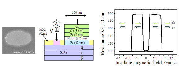 |
Fig.7 Magneto-resistance of Fe:MgO:Fe MTJ grown on p-i-n GaAs. Measurement setup and SEM image of contact with area 200 nmx200 nm are shown |
In commercial MRAM the thickness of free layer is about 2-3 nm. It is possible, but difficult to reduce the thickness of the free layer in our device till 2-3 nm. Usually, in the case of free-layer thickness thinner than 10 nm, MR ratio decreases and becomes zero for free-layer thickness thinner than 5 nm. As was measured by SIMS the reason for this is contamination of Fe free layer by As and Ga. We are constantly improving technology and reducing the contamination of free layer in order to reduce free-layer thickness.
The thickness of the free layer should be 2-3 nm.
In the following experiment I have tried to reverse the magnetization of the free layer by the injected photo-induced electrons into MTJ. The magnetization was not reversed, but there was a change of MR curve probably indicating magnetization precession. The magnetization precession occurs when the injected current is slightly below the threshold current for the magnetization reversal.
Figure 9 shows experimental setup. Light beam was focused in close vicinity of MTJ electrode. The photo-excited in p-i-n GaAs were injected into MTJ. The graph shows magneto-resistance of Fe:MgO:Fe MTJ measured when photo electrons are excited in p-i-n GaAs by 150-fs optical pulses for different energy of optical pulses. The magnetization of free layer has not been reversed, because the free-layer is still thick. However, there is a dependence of measured MR on the pulse intensity indicating precession of the magnetization of free layer. In the case of a MRAM cell such precession is usually observed when the current is slightly below the threshold current.
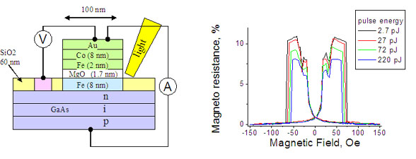 |
Fig.9 Magneto-resistance of Fe:MgO:Fe MTJ measured when photo-excited electrons are excited in p-i-n GaAs by 150-fs optical pulses and injected into the MTJ. |
Part 3. recording |
||||
|---|---|---|---|---|
|
I will try to answer your questions as soon as possible


 Video
Video 
