Dr. Vadym Zayets
v.zayets(at)gmail.com
My Research and Inventions
click here to see all content |

Dr. Vadym Zayetsv.zayets(at)gmail.com |
|
 |
classic model ofspin transportmodel of spin-down/spin-up bandsmore chapters on this topic:IntroductionBasic Transport equationsSpin and charge currentsSpin drainNon-magnetic metalsFerromagnetic metalsSemiconductors (Basic)Threshold spin currentSpin gain/dampingSpin RelaxationSpin Hall/ Inverse Spin Hall effectsee-interaction
classic model ofspin transportmodel of spin-down/spin-up bandsmore chapters on this topic:IntroductionBasic Transport equationsSpin and charge currentsSpin drainNon-magnetic metalsFerromagnetic metalsSemiconductors (Basic)Threshold spin currentSpin gain/dampingSpin RelaxationSpin Hall/ Inverse Spin Hall effectsee-interaction
classic model ofspin transportmodel of spin-down/spin-up bandsmore chapters on this topic:IntroductionBasic Transport equationsSpin and charge currentsSpin drainNon-magnetic metalsFerromagnetic metalsSemiconductors (Basic)Threshold spin currentSpin gain/dampingSpin RelaxationSpin Hall/ Inverse Spin Hall effectsee-interaction
classic model ofspin transportmodel of spin-down/spin-up bandsmore chapters on this topic:IntroductionBasic Transport equationsSpin and charge currentsSpin drainNon-magnetic metalsFerromagnetic metalsSemiconductors (Basic)Threshold spin currentSpin gain/dampingSpin RelaxationSpin Hall/ Inverse Spin Hall effectsee-interaction
classic model ofspin transportmodel of spin-down/spin-up bandsmore chapters on this topic:IntroductionBasic Transport equationsSpin and charge currentsSpin drainNon-magnetic metalsFerromagnetic metalsSemiconductors (Basic)Threshold spin currentSpin gain/dampingSpin RelaxationSpin Hall/ Inverse Spin Hall effectsee-interaction |
Spin and Charge Transport in Semiconductors Spin and Charge Transport in a semiconductor. Classical model of the spin-up/spin-down band.
|
|
|||
Fig. 1 Threshold spin current in the semiconductor. (a) Spin chemical potential, (b) spin selectivity and (c) density of accumulated electrons for diffusive spin current propagating along n-Si bar (doping concentration 1016 cm-3). The region of high spin/charge accumulation is from 0 to ~0.2 mm. The dash lines in (a) shows the case when spin current flow in a non-magnetic metal having the same spin diffusion length and the same conductivity. In cases (a) and (c), the scale of y-axis is logarithmic. |
To demonstrate this effect, we have solved numerically the set of spin/charge transport equations in a semiconductor by the Finite Difference Method (FDM) for an n-Si bar (mobility of 1450 cm2/V/s, spin diffusion length of 1 um, doping concentration of 1E16 cm-3). The Neumann boundary conditions of zero charge current and a given value of spin current were used as the boundary conditions at the left-side of the bar. Open-boundary conditions for the spin current and a zero value for the charge chemical potential were used as the boundary conditions at the right side of the bar. Figure 1 shows the calculated spin chemical potential ![]() , the spin selectivity beta and the accumulated electrons density. In the case when the input current is below 2 uA/um2 the spin selectivity beta and the charge accumulation are small and the spin diffusion in the semiconductor is almost the same as the spin diffusion in a non-magnetic metal. The decay of the spin current and the spin chemical potential
, the spin selectivity beta and the accumulated electrons density. In the case when the input current is below 2 uA/um2 the spin selectivity beta and the charge accumulation are small and the spin diffusion in the semiconductor is almost the same as the spin diffusion in a non-magnetic metal. The decay of the spin current and the spin chemical potential ![]() follow the exponential law with the effective spin diffusion length equal to the intrinsic spin diffusion length in the semiconductor. This corresponds to the straight dark-yellow line of Fig.1 (a). However, for larger magnitudes of the input spin current, the spin diffusion in semiconductors becomes different from the spin diffusion in non-magnetic metals and the region of high spin/charge accumulation is formed. The decay of spin chemical potential
follow the exponential law with the effective spin diffusion length equal to the intrinsic spin diffusion length in the semiconductor. This corresponds to the straight dark-yellow line of Fig.1 (a). However, for larger magnitudes of the input spin current, the spin diffusion in semiconductors becomes different from the spin diffusion in non-magnetic metals and the region of high spin/charge accumulation is formed. The decay of spin chemical potential ![]() deviates from the exponential law (red, blue, black lines of Fig. 1(a)). Inside the accumulation region, the spin charge accumulation is larger compared to the case of a non-magnetic metal. Outside this region the spin accumulation is smaller. As can be seen from Fig.1(c), the large spin accumulation is accompanied by a large charge accumulation.
deviates from the exponential law (red, blue, black lines of Fig. 1(a)). Inside the accumulation region, the spin charge accumulation is larger compared to the case of a non-magnetic metal. Outside this region the spin accumulation is smaller. As can be seen from Fig.1(c), the large spin accumulation is accompanied by a large charge accumulation.
The physical mechanism for the formation of a region of high spin/charge accumulation is explained as follows. As can be seen from Fig. 1(b) and Fig. 2(b), in case of a small input spin current, the spin selectivity beta in a semiconductor is small and it has a little influence on the transport. In the case when the input spin current exceeds 5 uA/um2, the spin selectivity beta approaches 100 % in the region close to the input. As has been shown here, in the case when the spin selectivity beta approaches 100 % the spin transport drastically changes. The effective spin length shortens, significant charge is accumulated and eventually spin diffusion stops. In a semiconductor, the spin selectivity beta increases with the increase of the magnitude of the spin current. Inside the region near the input where beta approaches 100%, the spin diffusion length significantly shortens, meaning that there spin diffusion practically stops. Only a small amount of spin current leaks from this region. Since spin current does not diffuse out of this region, more spin is accumulated there, causing an even larger beta and an even larger spin accumulation. Therefore, the process of spin/charge accumulation is avalanche-like. As can be seen from Figs.1(a) and Fig.2(a), when the input spin current increases further from 8 uA/um2 to 12 uA/um2, the amount of the spin current leaked from the accumulation region almost does not change. This means the spin current can not pass into the Si bar and so the majority of the spin current decays inside the spin/charge accumulation region.
Even though the explained effect limits the amount of spin current, which could pass through the semiconductor, the effect may be used in some applications. For example, the electron accumulation in the spin/charge accumulation region may significantly exceed the doping concentration in the semiconductor. This leads to a substantial increase of the conductivity of this region, meaning that a spin current may switch a semiconductor from a weakly-conductive state into a larger-conductivity state.
It should be noticed that the threshold spin current decreases with the decrease of the doping concentration and with the increse of the spin diffusion length.
In all examples, the animated parameter is the input spin current (shown on top of the figures).
Case A (threshhold spin current ~12 uA/um2)
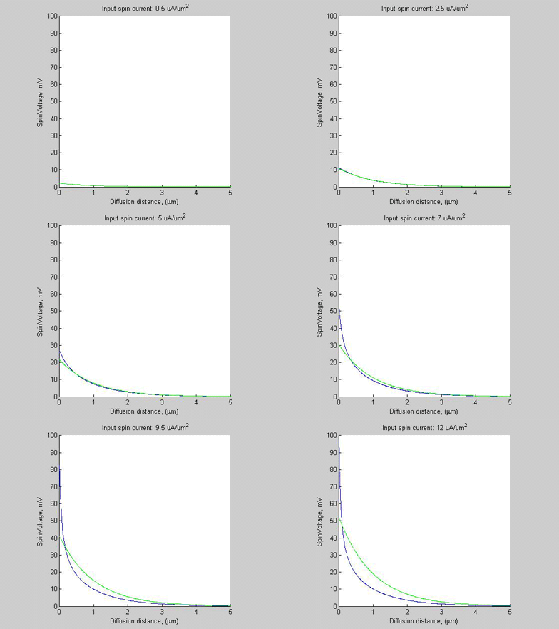
Temperature=300 K, mobility=1450 cm^2/V/s, Spin Diffusion Length= 1 um, Doping concentration 1E16 1/cm^3.
 |
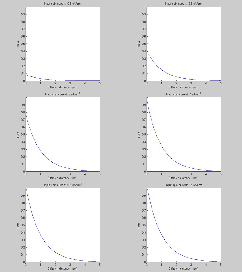 |
Fig.2a Case A. The spin chemical potential |
Fig.2b Case A. Spin selectivity beta. |
Figures 2a and 2b show the spin chemical potential ![]() and spin selectivity beta, respectively. In the case of small input spin current, the spin voltage and the beta are small and the spin voltage exponentially decreases along propagation distance. The spin diffusion in this case is very similar to the case of spin diffusion in a non-magnetic metal (beta=0) . In this case the spin chemical potential
and spin selectivity beta, respectively. In the case of small input spin current, the spin voltage and the beta are small and the spin voltage exponentially decreases along propagation distance. The spin diffusion in this case is very similar to the case of spin diffusion in a non-magnetic metal (beta=0) . In this case the spin chemical potential ![]() is linearly proportional to spin current.
is linearly proportional to spin current.
![]()
where ls and sigma are the spin diffusion length and conductivity, respectively.
As the input spin current increases, the![]() increases and beta approaches to 1 and a region of high spin/charge accumulation is formed. Ratio (1) is not valid for this region. Mostly all injected spin current is relaxed inside this region. Only a small amount of spin current is leaking from this region into the semiconductor.
increases and beta approaches to 1 and a region of high spin/charge accumulation is formed. Ratio (1) is not valid for this region. Mostly all injected spin current is relaxed inside this region. Only a small amount of spin current is leaking from this region into the semiconductor.
 |
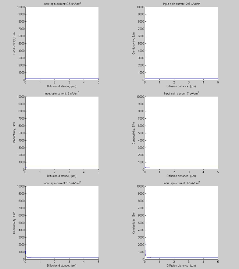 |
Fig.3 Case A. Charge accumulation |
Fig.4 Case A. Conductivity |
As was described here, in case of non-zero beta, the charge is accumulated along the diffusion of the spin current. The charge accumulation is proportional to the second derivation of the ![]()
![]()
Since in the spin accumulation region the![]() sharply decreases, the charge accumulation in this region is significant. Figure 3 shows the charge accumulation. In case when the input current is near the threshold current, the accumulated electron concentration induced by the spin current may significantly exceed the doping concentration in the semiconductor (See Fig.3).
sharply decreases, the charge accumulation in this region is significant. Figure 3 shows the charge accumulation. In case when the input current is near the threshold current, the accumulated electron concentration induced by the spin current may significantly exceed the doping concentration in the semiconductor (See Fig.3).
The conductivity of the semiconductors is linearly proportional to electron (hole) concentration. Figure 4 shows the conductivity. In the case when the input current is near the threshold current, the conductivity in the narrow spin/charge accumulation region is about one order larger than conductivity of outside of this region. It is because a significant elctron accumulation inside the spin/charge accumulation region. Therefore, the diffusive spin current can switch the semiconductor from a weakly-conductive state into a larger-conductivity state.
 |
 |
 |
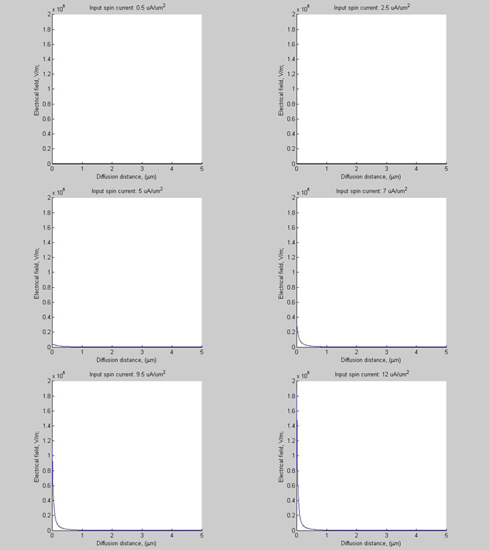
Fig.5 Case A. Electrical Field |
Fig.6 Case A. Electrical potential | Fig.7 Case A. Spin Current (blue line). Green line shows the imaginary case of beta=0 for comparison |
Since there is a large charge accumulation, there is also a significant build-up electrical field inside spin accumulation region (Fig.5) and electrical voltage (Fig.6).
The electrical potential difference between two sides of the semiconductor can be used to detect the magnitude of the spin current (For details about spin detection, click here). Figure 6 shows the electrical potential. The potential difference between two sides significantly enlarges when input spin current is near the threshold current.
Figure 7 demonstrates the effect of the spin/accumulation region on the spin current . It can be seen that when the spin/accumulation region is formed, only a small amount of the spin current leaks out of this region.
The only difference between Case A and Case B is the doping of Si. In the case B doping is an order larger than in the case A.
Case B(threshhold spin current ~95 uA/um2) (doping -> x10 times of case A, threshold current -> x8 times of case A)
Temperature=300 K, mobility=1450 cm^2/V/s, Spin Diffusion Length= 1 um, Doping concentration 1E17 1/cm^3.
 |
 |
 |
Fig.8 Case B. Higher doping. The spin chemical potential |
Fig.9 Case B. Higher doping. Charge accumulation | Fig.9a Case B. Higher doping. Spin Current |
Figure 8 shows the spin chemical potential ![]() for the case B. Comparing with the Case A, the threshold current is about one order larger, but it is still very small about 100 uA/um2. ( For example, to reverse magnetization in a MRAM cell the current density about 1E7 A/cm2=100 mA/um2 is required. The saturation current density in the case B is 0.1 mA/um2).
for the case B. Comparing with the Case A, the threshold current is about one order larger, but it is still very small about 100 uA/um2. ( For example, to reverse magnetization in a MRAM cell the current density about 1E7 A/cm2=100 mA/um2 is required. The saturation current density in the case B is 0.1 mA/um2).
Comparing Fig 1 and 8, for the current near threshold current the spin chemical potential does not depends on the doping concentration. In the both cases A and B, it is about 100 mV. However, the corresponding spin accumulation in case B is about one order of magnitude larger than in the case B. The same is valid for the charge accumulation. In the case B the charge accumulation may reach over 1E18 1/cm3. That is one order larger than Si doping concentration in the Case B. Therefore, even in the case of higher doping of a semiconductor, the modulation of electron concentration (conductivity) by a spin current still may be significant.
The only difference between Case A and Case C is temperature. It is assumed that the spin length is temperature independent.
Case C (threshhold spin current ~16 uA/um2, the change is not significant comparing with 300 K)
Temperature=70 K, mobility=10000 cm^2/V/s, Spin Diffusion Length= 1 um, Doping concentration 1E16 1/cm^3.
 |
 |
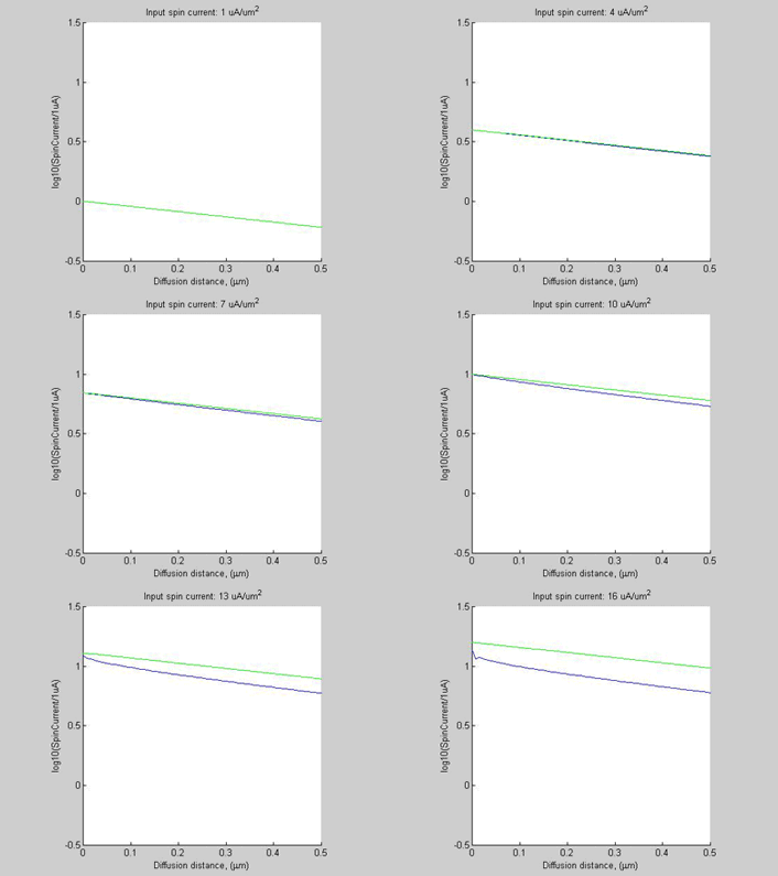 |
Fig.10 Case C. T=70 K.The spin chemical potential |
Fig.11. CaseC. T=70 K.Charge accumulation | Fig.12. CaseC. T=70 K.Spin current |
Comparing Cases A and C, the threshold current only slightly increases when the temperature decreases. It should be noticed that the spin chemical potential inside the spin accumulation region is about 3 times smaller in the case of T=70 K than in the case of room temperature. It is because, the beta more rapidly increases with the increase of the spin chemical potential at lower temperature (For details, see here)
The only difference between Case A and Case D is the spin diffusion length. In the case D the spin diffusion length is 10 times shorter than it is in the case A.
Case D (threshhold spin current =92 uA/um2) (spin diffusion length->1/10 of case A, threshold current -> x8 times of case A)
Temperature=300 K, mobility=1450 cm^2/V/s, Spin Diffusion Length= 0.1 um, Doping concentration 1E16 1/cm^3
 |
 |
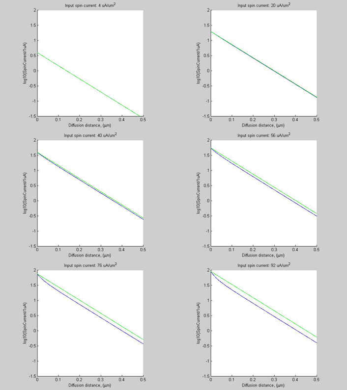 |
Fig.13 Case C. Shorter Spin diffusion length. The spin chemical potential |
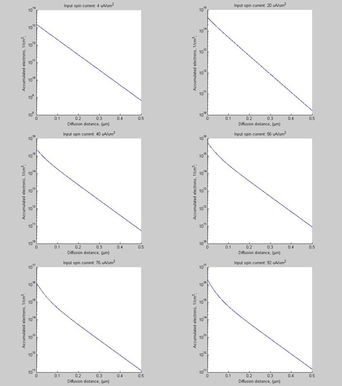
Fig.14. Case D. Shorter spin diffusion length.Charge accumulation | Fig.15. Case D. Shorter spin diffusion length. Spin current |
Besides the 8-time increase of he threshold spin current, the shortening spin diffusion length leads to about 10-time decrease of width of spin/charge accumulation region.
It is should be noticed that in all above calculations it was assumed that the spin diffusion length does not depend on the spin or charge accumulations. As was discussed here, both the spin and charge accumulations might significantly influence the spin diffusion length. This may influence a value of the threshold spin current.
I will try to answer your questions as soon as possible