Dr. Vadym Zayets
v.zayets(at)gmail.com
My Research and Inventions
click here to see all content |

Dr. Vadym Zayetsv.zayets(at)gmail.com |
|
|
classic model ofspin transportmodel of spin-down/spin-up bandsmore chapters on this topic:IntroductionBasic Transport equationsSpin and charge currentsSpin drainNon-magnetic metalsFerromagnetic metalsSemiconductors (Basic)Threshold spin currentSpin gain/dampingSpin RelaxationSpin Hall/ Inverse Spin Hall effectsee-interaction
classic model ofspin transportmodel of spin-down/spin-up bandsmore chapters on this topic:IntroductionBasic Transport equationsSpin and charge currentsSpin drainNon-magnetic metalsFerromagnetic metalsSemiconductors (Basic)Threshold spin currentSpin gain/dampingSpin RelaxationSpin Hall/ Inverse Spin Hall effectsee-interaction
classic model ofspin transportmodel of spin-down/spin-up bandsmore chapters on this topic:IntroductionBasic Transport equationsSpin and charge currentsSpin drainNon-magnetic metalsFerromagnetic metalsSemiconductors (Basic)Threshold spin currentSpin gain/dampingSpin RelaxationSpin Hall/ Inverse Spin Hall effectsee-interaction
classic model ofspin transportmodel of spin-down/spin-up bandsmore chapters on this topic:IntroductionBasic Transport equationsSpin and charge currentsSpin drainNon-magnetic metalsFerromagnetic metalsSemiconductors (Basic)Threshold spin currentSpin gain/dampingSpin RelaxationSpin Hall/ Inverse Spin Hall effectsee-interaction
classic model ofspin transportmodel of spin-down/spin-up bandsmore chapters on this topic:IntroductionBasic Transport equationsSpin and charge currentsSpin drainNon-magnetic metalsFerromagnetic metalsSemiconductors (Basic)Threshold spin currentSpin gain/dampingSpin RelaxationSpin Hall/ Inverse Spin Hall effectsee-interaction |
Semiconductors. Basic Equations.
Spin and Charge Transport. Classical model of the spin-up/spin-down band.
|
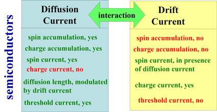 |
Fig.1 Properties of drift charge current and diffusion spin current in semiconductors. |
In a semiconductor the spin selectivity ![]() is not constant throughout the bulk of the material. At each point it is a function of the magnitude of the spin accumulation there. Because of this condition, there are several unique features of spin transport in semiconductors such as: a spin conversion between drift and diffusion currents; an existence of a threshold spin current; and a gain/damping of the spin current by a charge current.
is not constant throughout the bulk of the material. At each point it is a function of the magnitude of the spin accumulation there. Because of this condition, there are several unique features of spin transport in semiconductors such as: a spin conversion between drift and diffusion currents; an existence of a threshold spin current; and a gain/damping of the spin current by a charge current.
Below I will derive a set of equations, which describe the spin and charge transport in non-degenerate semiconductors. But I would like to start with a numerical example, which demonstrates similarities in spin transport in ferromagnetic metals and semiconductors. However, it should be noticed that the spin transport in semiconductors significantly more complex than the spin transport in ferromagnetic metals.
Spin-dependent conductivity in iron.
In ferromagnetic metals the number of conduction electrons with spin aligned along and opposite to the magnetization of metal is different. For example, we assume that 70 % of electrons participating in transport in iron have spin directed along the magnetization of Fe (spin-up) and 30 % of electrons have spin directed opposite to the magnetization of Fe (spin-down). The conductivity of iron is 1.12e7 S/m. The conductivity is linearly proportional to the number of electrons participating in the transport. Assuming that the difference of mobility for spin-up and spin-down electrons in iron is small, the conductivity of spin-up electrons is 0.7*1.12e7 S/m=7.84e6 S/m and the conductivity of spin-down electrons is 0.3*1.12e7 S/m=3.36e6 S/m. The conductivity of spin-up electrons is approximately 2 times larger than the conductivity of spin-down electrons. The difference of conductivities for spin-up and spin-down electrons determines unique features of the spin transport in iron.
Spin-dependent conductivity in silicon.
For example, let us consider the case of n-Si with doping concentration of 4e16 1/cm3 and mobility of 1450 cm2/V/s at room temperature when approximately all dopants are ionized. Conductivity of silicon=q*mobility*number_of_electrons=1.6E19 C*1450 cm2/V/s*4e16 1/cm3=930 S/m. In the case when there is no spin accumulation in the silicon, the number of spin-up electrons of 2e16 1/cm3 and the number of spin-down electrons of 2e16 1/cm3 are equal. Also, the conductivity is the same for spin-up and spin-down electrons and it equals 465 S/m =930/2 S/m. Of course, the conductivity in this case is spin independent.
Next, let us consider the case when there is a spin accumulation in the silicon, but there is no charge accumulation. For example it could be a case, when illuminating the silicon by circularly polarized light we have turned up the spin direction of 90 % percent of spin down electrons. In this case the number of spin-up and spin-down electrons is 1.9*2e16 1/cm3=3.6e16 1/cm3 and 0.1*2e16 1/cm3=2e15 1/cm3, respectively. The corresponded conductivity of the spin-up and spin-down electrons is 836 S/m and 46 S/m, respectively. Therefore, the conductivity of spin-up electrons in this silicon is 18 times larger the conductivity of spin-down electrons (comparing to only 2 times in the previous example of iron). Therefore, intuitively it could be understood that all unique features of spin transport, which exist in iron, should also exist in the silicon.
It is important to notice that in a semiconductor the conductivity is spin-dependent only when there is a spin accumulation in it. In a ferromagnetic metal, the conductivity is always spin-dependent.
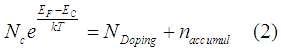
In the case of a non-degenerate n-type semiconductor, the number of electrons in the conduction band is
![]()
where ![]() are the effective density of states in the conduction band, the Fermi energy and the energy of the bottom of the conduction band, respectively. In a semiconductor both the charge and spin can be accumulated. In the case when there is a charge accumulation, the number of electrons in the conduction band is
are the effective density of states in the conduction band, the Fermi energy and the energy of the bottom of the conduction band, respectively. In a semiconductor both the charge and spin can be accumulated. In the case when there is a charge accumulation, the number of electrons in the conduction band is
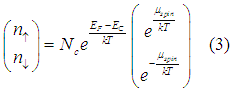
where ![]() are the doping concentration and the concentration of accumulated electrons, respectively. In the case when additionally there is a spin accumulation, the number of spin up and spin-down electrons in the conduction band is
are the doping concentration and the concentration of accumulated electrons, respectively. In the case when additionally there is a spin accumulation, the number of spin up and spin-down electrons in the conduction band is
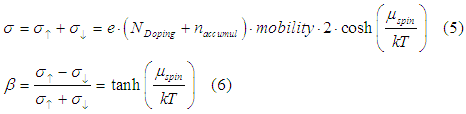
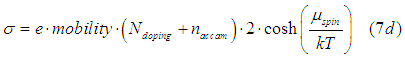
Noticing that in non-degenerated semiconductor the mobility only weakly depends on charge and spin accumulations, the conductivity for spin-up and spin-down electrons can be calculated as
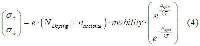
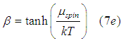
The effective conductivity sigma and spin selectivity beta in a semiconductor are calculated from (4) as
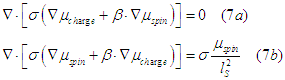
In contrast to ferromagnetic and non-magnetic metals, where the spin selectivity beta is a constant throughout the bulk of the metal, in a semiconductor the spin selectivity beta depends on the magnitude of spin accumulation. Therefore, in semiconductors the beta satisfies
![]()
The condition (7) determines unique spin-transport properties of semiconductors such as: spin conversion between a drift and diffusive currents; existence of a threshold spin current and gain/damping of the spin current by a charge current.
The spin and charge transport in semiconductors is described by a following set of five equations (7(a)-7(e))
Spin/Charge transport equations
Gauss's law
![]()
conductivity
spin selectivity
which has 5 unknowns: ![]()
The equations of the set (7) are non-linear and in general they should be solved numerically.
Once again in semiconductors the spin and charge transport are described by the following set of 5 equations
In 2002 Dr. Scott A. Crooker studied spin accumulation in GaAs at low temperature by Kerr rotation technique (New Journal of Physics 9 (2007) 347). The spin accumulation was excited by a circulary polarized laser beam and it was focused into a 5-um-diameter spot. Space distribution of the spin accumulation was measured by Kerr rotation of a scanning probe beam.
Without an applied electrical field, there was an exponential decay of spin accumulation out of the excited laser beam (Fig.2a of Ref. ). It was well expected. When an electrical field was applied the spin accumulation was shifted toward the direction of the electrical field (Fig.4a of Ref. ). It looked like the spin accumulation was drifted by the applied electrical field. It was a very surprised result. The spin accumulation is an uncharged object and uncharged object should not be drifted by an electrical field. As was explained here, generally a diffusion spin current and a drift charge current flow independently without interaction and electrical field should not influence the spin diffusion.
However, a semiconductor is a special material. There is a significant interaction between drift and diffusion spin currents in the semiconductors. As shown here, in a semiconductor the spin diffusion length elongates when diffusion and drift currents flow in the same direction and the spin diffusion length shortens when the flows in the opposite directions. This fact well explains the data of Fig.4a of Ref.. The applied electrical field induces a drift current from left to right (which is invisible for the Kerr measurements). Due to the interaction of a diffusive spin current with a drift current, the spin diffusion length shortens for diffusion current flows from right to lift and it elongates for the flow from left to right. Therefore, the shape of spin accumulation becomes elliptical with the elongation towards left.
Above facts well explain the data of Fig.4a of Ref. without violating the fact that uncharged object should not be drifted by an electrical field.
Also, it should be noticed that this effect is unique for semiconductors only. It will not occur in metals.
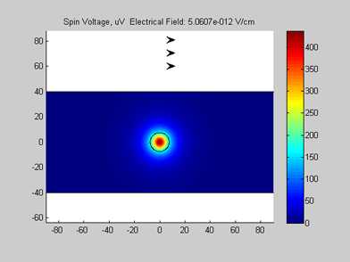 |
Fig.1 Animated picture. Spin chemical potential |
The data of Fig.4a of Ref. were simulated by the full set of charge/spin transport equation for electrons (7) for n-GaAs at T=10 K. GaAs thickness is 1 um, mobility is 4000 cm2/V/s (low?), spin length 10 um, doping is 1E16 1/cm3.
Gaussian-shape circulary-polarized 5-um-dimeter laser beam (power 5 uW) excites spins accumulation in GaAs. The reflectivity of GaAs is 32 %. It is assumed 50 % spin conversion efficiency, because there is no splitting between heavy and light holes. Details are here.
Calculation 1.
In order to clarify the spin transport in the Calculation 1, at first I have ignored in calculation the photo-excited holes and electrons. I assume that the laser beam is only a spin source, but it is not source of photo-excited electrons and holes.
Figure 1 shows the spin chemical potential ![]() . The measured Kerr rotation angle is linearly proportional to
. The measured Kerr rotation angle is linearly proportional to ![]() . There is a good match between experimentally measured and calculated data.
. There is a good match between experimentally measured and calculated data.
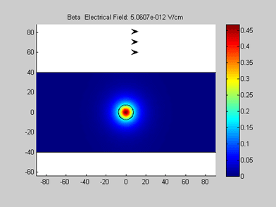
Figure 2 show the spin selectivity beta. The beta is largest near the center of the laser beam and it can reach 45%. It is high (almost the same value as in Fe), but it is not high enough to see the effect of a threshold spin current and the blocking of spin diffusion. When the electrical field is applied, the beta is decreasing.
Figure 3 show the accumulated charge density. The maximum accumulated charge density is about 1.5E10 1/cm3, which is significantly smaller than the doping concentration of n-GaAs (1E16 1/cm3). It is another indication that the spin current is still far from the threshold spin current. It should be noticed that there positive and negative charge accumulation. Of course, the integrated accumulated charge is zero.
 |
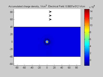 |
Fig. 2. Animated picture. Spin selectivity beta. Animated parameter is the magnitude of applied electrical field. |
Fig.3 Animated picture. Charge accumulation due to spin diffusion. Animated parameter is the magnitude of applied electrical field. |
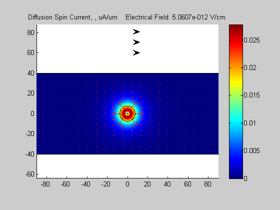
Figures 4 and 5 show diffusion and drift spin currents. Far away from the laser beam the drift current is not spin-polarized. Whet it enters the region of spin accumulation, it becomes spin-polarized, because in this region the conductivity is spin dependent (See Fig. 2).
Under applied electrical field, the distribution of the diffusion. current is not of an elliptical shape. Perhaps, it is because the effect of diffusion blocking near threshold spin current starts to influence the diffusion.
 |
 |
Fig.4 Animated picture. Diffusion spin current. The arrows show the direction of the current. Animated parameter is the magnitude of applied electrical field. |
Fig. 5. Animated picture. Drift spin current. The arrows show the direction of the current. Animated parameter is the magnitude of applied electrical field. |
I will try to answer your questions as soon as possible

 It is important!!!! All data on this page are calculated based on the model of the spin-up/spin-down bands. The model of the spin-up/spin-down bands ignores
  For the modified model, which includes all above-mentioned facts,