Dr. Vadym Zayets
v.zayets(at)gmail.com
My Research and Inventions
click here to see all content |

Dr. Vadym Zayetsv.zayets(at)gmail.com |
|
|
Surface Plasmons
IntroductionOur goal is to fabricate an efficient optical isolator utilizing an plasmonic waveguide. In a plasmonic waveguide with a ferromagnetic metal the magneto-optical (MO) effect can be significantly enhanced. The MO enhancement occurs near cutoff conditions for optical plasmons.Technology of plasmonic waveguidesIn a plasmonic waveguides a metal is used to guide light. Any metal significantly absorbs light. Therefore, a design and a fabrication technology is critically important for a plasmonic waveguide. 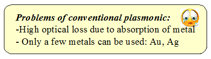 Conventional technology -> high plasmon propagation loss Plasmonic waveguide= a stripe of metal on dielectric or a stripe of photoresist (dielectric) on metal Only a few metals can be used. Only Au or Ag are used as a metal It is not easy to integrate such technology into the Photonic Integrated Circuits (PIC)
Optimized technology -> low plasmon propagation loss
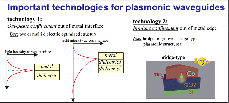
Almost any metal can be used and a low plasmon propagation loss can be achieved. The magneto-optical, electro-optical and non-linear effects can be significantly enhanced. Two key technologies for a plasmonic waveguide: Technology 1. Out-plane confinement out of metal interface Details of this technology are here In a simple case of a a metal on single-layer dielectric, light intensity in dielectric sharply decreases out of the metal interface. Therefore, there is a lot light inside of the metal and the plasmon propagation loss is large. In a case of a a metal on optimized double- or multi-layer dielectric, light intensity decreases slowly deep into dielectric. Therefore, there is a lot light is inside of the dielectric, but only a tiny amount inside the metal. It makes the plasmon propagation loss small.
Technology 2. In-plane confinement out of metal edge Details of this technology are here A metal has a large difference in refractive index with a dielectric. Such large difference causes a light scattering even at a moderately- rough metal-dielectric interface. Often the contribution of this loss into a propagation loss of a plasmon is large than the contribution due to absorption by the metal. An effective confinement of plasmon out of metal edges is critical to achieve a small plasmon propagation loss especially in case of plasmonic waveguides of a smaller size.
Optical isolator for fiber-optics linksAt present there is a closed-to-perfect optical isolator made of magnetic garnets. The performance of the bulk isolator is nearly excellent, at present it is unfeasible that an isolator integrated into OIC would reach similar performance.Note: The optical isolator is the fourth most used element of optical networks (after the fiber, the laser diode and the photodetector) .The performance of an optical isolator is characterized by 3 main parameters: the isolation ratio, the insertion loss and the operational wavelength bandwidth. At present, the bulk-type optical isolator is commercially available. The structure of the bulk-type optical isolator is rather simple. It consists of a magnetic garnet inserted between two polarizers. Since both magnetic garnets with low absorption and the polarizers with low insertion loss and high extinction ratio are available, the performance of the present commercial optical isolator is close to perfect. The optical bulk isolators with isolation ratio of 40 dB, insertion loss of 0.7 dB and bandwidth of 20 nm are commercially available. Optical isolator for PICNote: the optical isolator is one of the few optical components, which has not yet been integrated into commercial PIC.The integration of optical elements into Photonic Integrated Circuits (PIC) is an important task, because it may reduce a cost and improve performance of high-speed optical data processing circuits for the high-speed optical networks. The integration of an optical isolator is important for OIC, because the problem of back-reflected light is more severe in the case of integrated optical elements. However, the optical isolator is one of the few optical components, which has not yet been integrated into commercial PIC. At present, there is a strong industrial demand for the integrated optical isolator. It should be noticed that since the performance of the bulk isolator is nearly excellent, at present it is unfeasible that an isolator integrated into PIC would reach a similar performance. For the merit of the integration, some penalties should be paid. Therefore, some parameters of the integrated isolator should be compromised. For example, in the case when the operational wavelength bandwidth may be compromised, a ring-type isolator may be a good option [1,2]. The ring-type isolator has very narrow bandwidth of about 0.01 nm.
Why it is difficult to integrate the optical isolator into PIC?Note: High crystal quality is required for garnets and diluted magnetic semiconductors in order to have the high Faraday rotation and the low optical loss. It is difficult to keep the high crystal quality during the fabrication of PIC.It is difficult to integrate the optical isolator into PIC for the following reason. The indispensable component of any optical isolator is a magneto-optical (MO) material. Traditionally, the magnetic garnets are used as a transparent MO material. However, it is difficult to grow the high-crystal-quality magnetic garnets on semiconductors substrates such as Si, GaAs, InP, which are used as a substrate for PIC, because the conventional growth temperature of the garnets is above the melting temperature of these substrates. To overcome this problem several solutions have been proposed. A wafer bonding between garnets and semiconductors and sputtering of garnet on Si were successfully used to fabricate the isolator on a Si substrate. Also, diluted magnetic semiconductors CdMnTe and CdMnHgTe have been used for the fabrication of optical isolator on a GaAs substrate. Even though a good performance of the above-mentioned standalone isolators fabricated on the semiconductor substrates were achieved, the integration of the isolators with other optical elements on the same substrate has not been demonstrated yet. The integration is difficult, because MO and optical properties of the garnets and diluted magnetic semiconductors (DMS) significantly depend on their crystal quality. As the crystal quality of garnets or DMS degrades, the MO constants in these materials are reduced and the optical loss is increased. Even if it is possible to keep a high crystal quality of the MO material during the fabrication of a standalone isolator, the crystal quality usually degrades during the fabrication of other elements of PIC. That is the reason why there are still difficulties to integrate a garnet-based isolator or a DMS-based isolator into a commercial PIC.
Ferromagnetic metal as a magneto-optical material??Note: From all known materials magneto-optical effect in the ferromagnetic metals is the largest. However, the optical absorption in the ferromagnetic metals is very large as well (Even about 10 times larger that the absorption in Au, Ag, Al and Cu)Ferromagnetic metals are attractive as an MO material for the optical isolator. They have very large MO constants and importantly they are technologically compatible with the fabrication technology of PIC. For the ferromagnetic metals the conventional sputtering and lift-off techniques may be used. They do not degrade during the fabrication of other optical components of PIC. There is one significant demerit of the ferromagnetic metals. They significantly absorb light. To overcome this problem, the design of an isolator, in which the optical absorption by a ferromagnetic metal is compensated by an optical gain of a semiconductor optical amplifier, has been proposed and realized . This type of isolator provides high isolation and has low optical insertion loss. However, the required operational pump current for this isolator is very high. At present, it is about 100 mA. The required current is unacceptably high for PIC. That is a reason why this type of isolator has not been integrated into PIC as well. The surface plasmons for the optical isolator ??Note: The plasmonic isolator can not compete with the bulk garnet-made optical isolator.Note: The technological compatibility with the fabrication technology of PIC and a wide operational wavelength bandwidth are major merits of the plasmonic isolator comparing to another designs of the integrated optical isolator.The surface plasmons intrinsically have a substantial optical loss. It is unlikely that the insertion loss and the isolation ratio of the plasmonic isolator would be the same as those of the bulk isolator. However, the ferromagnetic metals have very low wavelength dispersion of the optical and MO constants and the plasmonic isolator might be a good option for the integrated isolator when a wide operational wavelength bandwidth is required. Also, for the fabrication of the plasmonic waveguides the conventional sputtering and lift-off techniques may be used and the high-crystal quality of materials is not required in order to get high magneto-optical effect in magneto-optical waveguides. The technological compatibility with PIC fabrication technology is another important merit of the plasmonic isolator.
General facts about magneto-optics (MO) effect for plasmons are here Enhancement of MO effect in a double-dielectric plasmonic waveguide (general fact are here and examples are here, here and here) Experimental confirmation of low optical loss in Fe:SiO2:AlGaAs waveguide is here Cutoff condition for dielectric and plasmonic waveguidesDue to the optical confinement, light is guided along an optical waveguide. In the case of a dielectric waveguide, the optical confinement is achieved by a higher-refractive-index core layer. In the case of a plasmonic waveguide, it is achieved by a negative-refractive-index metallic layer. For a realistic applications of the plasmonic waveguides, a dielectric waveguide should be used to couple light in and out of the plasmonic waveguide ( experiment is here). For efficient coupling of light between a dielectric and plasmonic waveguides, the distribution of optical field in the plasmonic and dielectric waveguides should be very similar. It is only possible in the case when the dielectric waveguide is near cutoff condition. Here I study cutoff condition in AlGaAs dielectric waveguide(at lambda=750 nm here and at lambda=1500 nm here) and Si wire waveguide. These examples give a good idea how the optical confinement is weakened and eventually disappears at the cutoff.
Plasmonic slab waveguides
In the slab plasmonic waveguide there is is no in-plane confinement. All optical and MO properties of this plasmons can be found from the rigourous solution. Examples: 1. Plasmonic slab waveguide on GaAs substrate (lambda=800 nm) 2. Plasmonic slab waveguide on GaAs substrate (lambda=1550 nm) 3. Plasmonic slab waveguide on Si substrate (lambda=1550 nm)
|
I will try to answer your questions as soon as possible