Dr. Vadym Zayets
v.zayets(at)gmail.com
My Research and Inventions
click here to see all content |

Dr. Vadym Zayetsv.zayets(at)gmail.com |
|
|
IntroductionSi nanowire fabrication technology fiber/waveguide coupling setup integration: plasmonic + Si waveguides Out-plane plasmonic confinement AlGaAs waveguide (800 nm)in-plane confinement of plasmons
IntroductionSi nanowire fabrication technology fiber/waveguide coupling setup integration: plasmonic + Si waveguides Out-plane plasmonic confinement AlGaAs waveguide (800 nm)in-plane confinement of plasmons
|
Comparison of two technologies of Integration of Si nanowire waveguide and plasmonic waveguide Technology
|
Technology 1: Using a lift-off technique |
||||||||||||||||||
|
||||||||||||||||||
This technology can be only use when a Si-nanowire and plasmonic waveguide are connected in series. It cannot be used in the cases of parallel or side connections. |
||||||||||||||||||
| click on image to enlarge it |
(1) A thicker plasmonic structure can be used (thicker than 100 nm)
(2) Technology process is simpler.
(3) Protection of Si waveguides during the fabrication of plasmonic parts. All non- plasmonic part is covered by resist and remains fully intact during the fabrication of the plasmonic part.
(1) Moderate coupling loss between Si nanowire and plasmonic waveguides.
(2) A rough edge of the plasmonic section. It causes a subtantial scattering and a high plasmon propagation loss. In order to avoid high propagation loss, light is removed from the edges by in-plane confinement (See above)
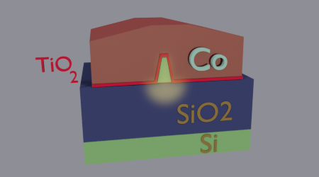
![]() Achievements on integration a magneto-optical plasmonic waveguide with a Si-nanowire waveguide (as 2019.04)
Achievements on integration a magneto-optical plasmonic waveguide with a Si-nanowire waveguide (as 2019.04)
![]() (1) low propagation loss: 0.7 dB/μm
(1) low propagation loss: 0.7 dB/μm
![]() (2) moderate coupling efficiency between the plasmonic and Si waveguides: 4 dB/facet
(2) moderate coupling efficiency between the plasmonic and Si waveguides: 4 dB/facet
It does not fit to a key requirement for the total insertion loss of a plasmonic device to be less than 3-5 dB.
 Technology flow:
Bridge-type plasmonic See Click on image to enlarge it |
 |
Si nanowire waveguide (450-nm wide) are connected by bridge waveguide. The width of Si bridge is 100 nm. It is cover by a thin metal
|
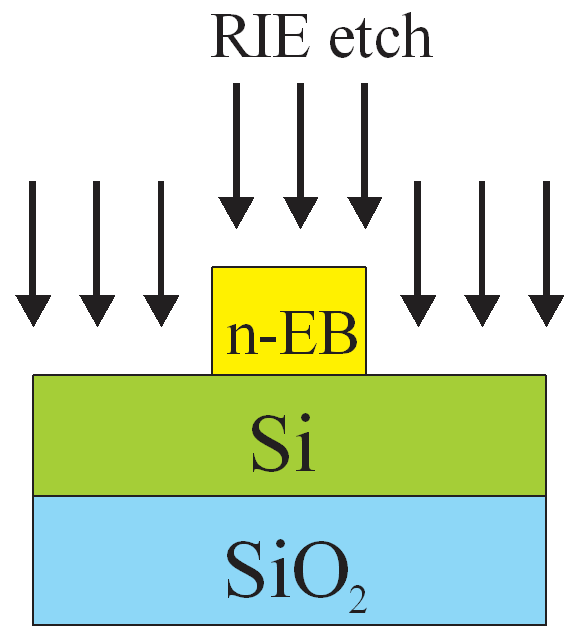
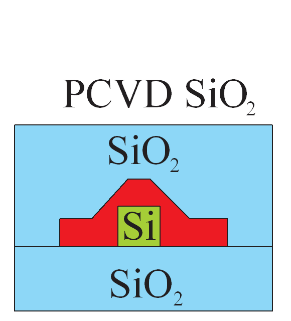
Starting wafer: SOI wafer (Si thickness is 220 nm) covered by 50-nm SiO2 (hard mask) and with Cr/Au/Cr alignment masks.
A negative thick EB resist is used ( resist thickness ~ 100 nm) . A negative resist means that parts, which was exposed to the EB beam, is not etched. Si nanowire waveguide width is 450 nm. The width of the spot-size converter is 150 nm. The width of Si-bridge of plasmonic part is 50 nm (70 nm is also OK).
RIE dry etch of SiO2 hard mask and Si following by a short wet etching of Si and etching out of remains of SIO2 hard mask
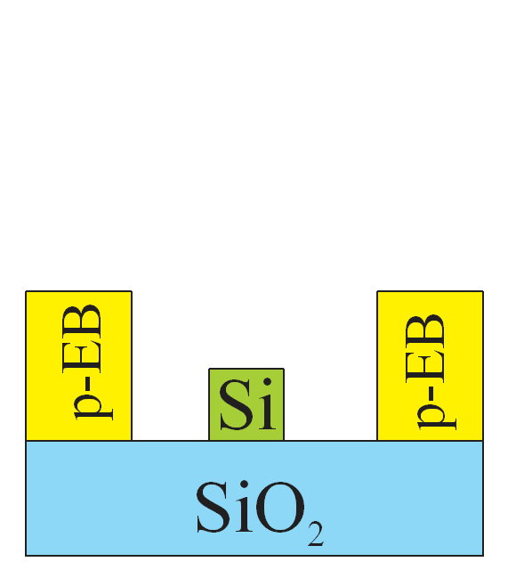
LAL (1000 nm) layer + positive resist. A negative resist means that parts, which was exposed to the EB beam, are etched out. The LAL layer is used in order to simplify the lift-off and improve the etch smoothness of the plasmonic part
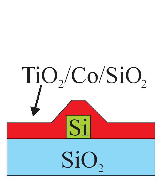
Sputtreing of
SiO2 (100 nm) . Purpose: to aligh
Technology 2: without use of a lift-off technique |
||||||||||||||||||
|
||||||||||||||||||
|
||||||||||||||||||
| click on image to enlarge it |
(1) A low coupling loss between Si nanowire and plasmonic waveguides.
(2) A side coupling and parallel coupling can be used.
(3) A smoother edge of the metal of the plasmonic structure. As a result, a plasmon may propagate at the edge of plasmonic structure (side coupling)
(1) Complexity of the fabrication technology
(2) Only a thin (<80 nm) plasmonic structure can be used due to the limitation of the deepest etching of the Ar-milling
(3) Severe alignment requirements.
(4) A slight destruction (a possible damaging) of non- plasmonic part. In this technology, a metal is deposited on unprotected non- plasmonic part. Next, the metal is etched out. Any imperfections of the technology
![]() Achievements on integration a magneto-optical plasmonic waveguide with a Si-nanowire waveguide (as 2019.04)
Achievements on integration a magneto-optical plasmonic waveguide with a Si-nanowire waveguide (as 2019.04)
The total insertion loss of a plasmonic waveguide coupled to a Si nanowire waveguides (bending radius=100 μm) is:
![]() 0.9 dB for gap width of 600 nm between Si and plasmonic waveguides
0.9 dB for gap width of 600 nm between Si and plasmonic waveguides
![]() 2 dB for gap width of 250 nm between Si and plasmonic waveguides
2 dB for gap width of 250 nm between Si and plasmonic waveguides
It fits to a key requirement for the total insertion loss of a plasmonic device to be less than 3-5 dB only in the case of the wide gap.
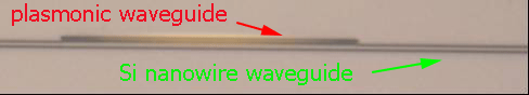
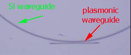
Side coupling of plasmonic waveguide and Si nanowire waveguide |
||
|
Fabrication technology of plasmonic waveguides |
|---|
| Thsi is my invited talk at SPIE Photonic West 2022 |
| YouTube video |
I will try to answer your questions as soon as possible