Dr. Vadym Zayets
v.zayets(at)gmail.com
My Research and Inventions
click here to see all content |

Dr. Vadym Zayetsv.zayets(at)gmail.com |
|
|
IntroductionSi nanowire fabrication technology fiber/waveguide coupling setup integration: plasmonic + Si waveguides Out-plane plasmonic confinement AlGaAs waveguide (800 nm)in-plane confinement of plasmons
IntroductionSi nanowire fabrication technology fiber/waveguide coupling setup integration: plasmonic + Si waveguides Out-plane plasmonic confinement AlGaAs waveguide (800 nm)in-plane confinement of plasmons
|
Plasmonic isolator
TechnologyOptical isolator is device, which is transparent in one direction and its blocks the light in opposite direction. Its function is similar to the diode in the electronics.
Why the integrated optical isolator is important?
The integration of different optical elements on one substrate is important to make the Photonic Circuits to be more cheaper and to have more functions. In a case of a dense integration the undesirable and unavoidable back reflection between different optical elements can severely disturb the operation of the Photonic Circuit. The back reflection can be suppressed by an optical isolator integrated between optical elements. At present, the most of optical elements (laser, detector, switch, modulator, amplifier) can be integrated in the Photonic Integrated Circuit(PIC), but not the isolator Why the integration of the optical isolator is difficult?Any design of the optical isolator should use a magneto-optical material. Only a magneto-optical material may have different optical properties What is the plasmonic isolator?The plasmonic isolator uses the unique non-reciprocal properties of plasmons, which propagates on a surface of a ferromagnetic metal. The plasmonic isolator benefits from large magneto-optical constants of a ferromagnetic metal and the ability of a substantial enhancement of the magneto-optical effect using a plasmon (see here and here). What are demerits of the plasmonic isolator?(1) Unavoidable part of the plasmonic isolator is a metal, which absorbs light. Therefore, some insertion loss is unavoidable for the plasmonic isolator. (2) In order to minimize the insertion loss, the length of the plasmonic isolator should be shorten. It limits the maximum isolation ratio the plasmonic isolator may provide. Maybe it is limited by 10 dB. The conventional bulk isolator provides 30 dB of the isolation. What are merits of the plasmonic isolator?(1) a small size.
(2) fabrication technology, which is well-compatible with the PIC
(3) a wide wavelength operational bandwidth
|
 |
| Plasmonic isolator |
| click on image to enlarge it |
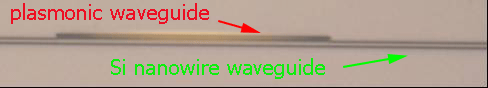
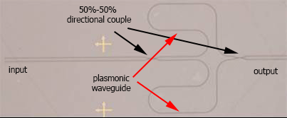
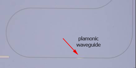
1) Type1: plasmonic waveguide blocks the direct propagation of light from input to output (See Fig.1)
2) Type 2: plasmonic waveguide in the vicinity of dielectric waveguide
In this case the plasmonic waveguides blocks the light propagation in Si nanowire waveguides. Light can reach output only in a case when a plasmon is excited. (See Fig. 1 and Fig.2)
Technology:
- Wedge-, bridge- or grove- types of plasmonic waveguides should be used. The confinement by a metal stripe should be avoided.
-Lift-off process can be used for a metal microfibrication .
Merits:
- Properties of a plasmon (MO effect, electro-optical effect) significantly influence the output light, because light can reach output only by excitation of a plasmon
Difficulties:
- Coupling efficiency between plasmonic and Si waveguides should be maximized (difficult)
-Propagation loss of plasmon should be minimized
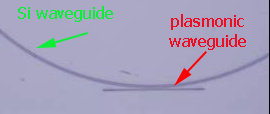
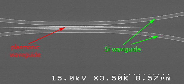
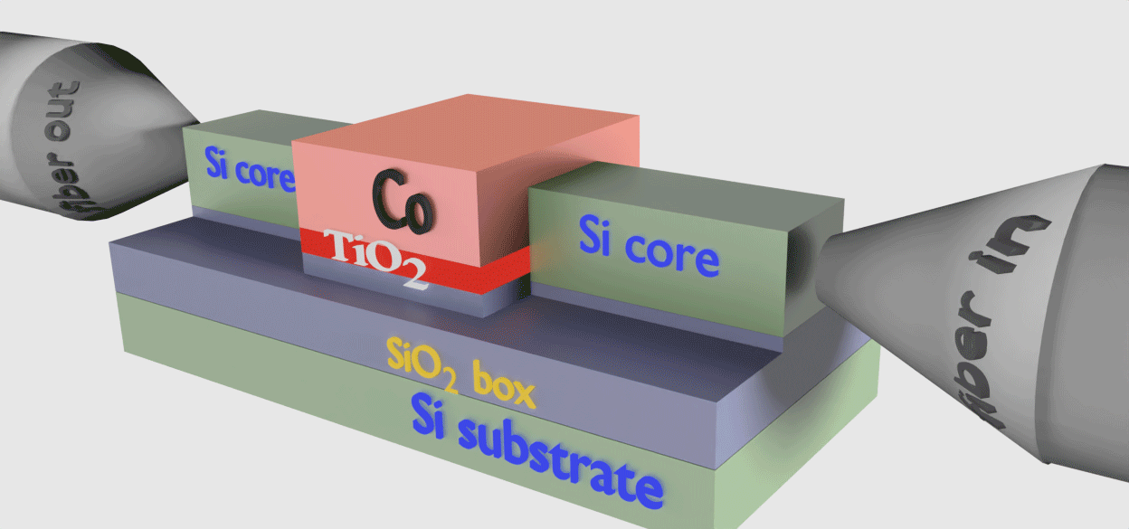
Fig.2 Plasmonic isolator Co/TiO2/SiO2 integrated with Si nanowire waveguides. Set with different lengths of plasmonic waveguides click on image to enlarge it |
 |
|
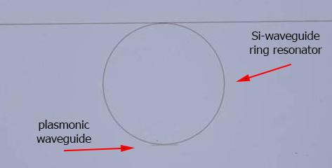
Plasmonic waveguide near Si nanowire waveguide |
||
|
In this case the plasmonic waveguides is integrated aside of a Si waveguide and the direct propagation of light is not blocked in Si waveguide. Only a resonance coupling in/out of a plasmonic waveguide only affects the output. It is similar to a ring resonator, where a ring is fabricated aside of a straight Si waveguide.
Technology:
- The etching by the Ar-milling should be used for for a metal microfibrication. The lift-off process should be avoided
-A combination of bridge-type and metal-stripe type of a plasmonic waveguide should be used.
Merits:
- A high coupling efficiency between plasmonic and Si waveguides is not as critical as in the case of the serial integration
-A low propagation loss of plasmon is not as critical as in the case of the serial integration.
Difficulties:
- - Unique properties of a plasmon (MO effect, electro-optical effect) affect only a little the output light. The influence is stronger only in a case of a resonance coupling of light into the plasmonic waveguide.
-
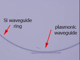
Ring resonator with plasmonic waveguide under it |
||
|
||
Under the ring of Si-waveguide-made ring resonator, there is a magneto-optical plasmonic waveguide. The resonance wavelength can be changed by reversing the magnetic field or by reversing light propagation direction (exchange the output and input) |
Mach–Zehnder interferometer with a plasmonic waveguide under each arm |
|||||
|
|||||
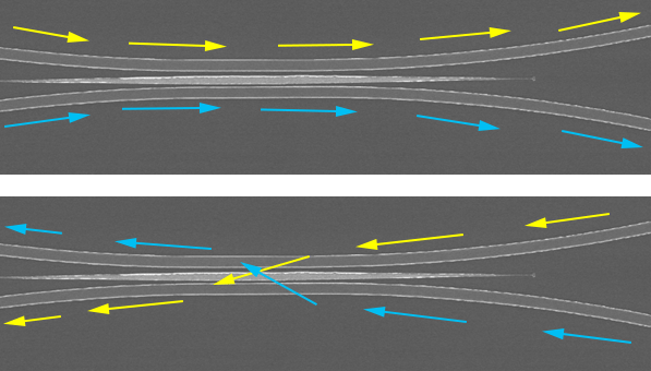
Under each arm of the Mach–Zehnder interferometer there is a plasmonic waveguide. The right figure shows direction of light propagation (yellow arrows). The blue arrows show the magnetization direction of a magneto-optical plasmonic waveguide. In respect to light propagation direction the magnetization is direct to right for light in the upper arm and to left in the lower arm. |
The input light is split into half and half by the first directional coupler. One half passes the upper arm and another half to the lower arm. The light combines by the second coupler. The output depends on the phase difference between the upper and lower arms.
Operational principle. Mach–Zehnder interferometer with a plasmonic waveguide under each arm |
|||||||||
|
|||||||||
| click on image to enlarge it |
Non-reciprocal directional coupler |
||
|
||
Inside of the gap of the non-reiciprocal coupler there is a magneto-optical plasmonic waveguide. The yellow and blue arrows show the light propagation direction for light coupled to different inputs. Because of the non-reciprocal properties of the plasmonic waveguide, the coupling efficiency is different for opposite propagation directions of light. |
I will try to answer your questions as soon as possible


 Comparing to other designs of the integrated isolator, the plasmonic isolator may not provide the largest isolation and may not have a smallest insertion loss, but a very small size, a simple and compatible fabrication technology and a wide wavelength operational bandwidth makes the plasmonic isolator a good fit for the integration into the PIC