Dr. Vadym Zayets
v.zayets(at)gmail.com
My Research and Inventions
click here to see all content |

Dr. Vadym Zayetsv.zayets(at)gmail.com |
|
|
Si nanowire waveguide. Basic properties.
Si wire waveguides (wavelength=1550 nm)Si nanowire waveguides are main part of any modern Photonic Integrated Circuit (PIC). They are used to connect all optical elements to each other. Their function is similar to the function of an electrical wire in an electronic circuit. Typically, the thickness of Si nanowire waveguide is 220 nm, the width is 440 nm (in range 400 nm-450 nm). The Si nanowire waveguides are fabricated on a SOI wafer using either an EB lithography or by a photolithography based on a ArF- type excimer laser (a ArF- stepper). A minimum resolution of the fabrication is defined by the required width of the spot size converter of 140 nm.page created in 2015, Modified in 2021.(note) The fabrication technology of a Si nanowire waveguide waveguide is very matured now. The intention of this page is to list well known facts, which could be helpful for engineering of photonic devices based on Si nanowire waveguidesResults in short.
(main result): The Si nanowire waveguide are the best waveguide (at least from which I have measured). A very low optical propagation loss, strong confinement and a very good fiber-to-waveguide coupling efficiency (about 2.5-3 dB) are distinguish features of the Si nanowire waveguides 1. Decrease of thickness or width of Si wire weakens confinement of waveguide mode. At the cutoff, the confinement is not sufficient to guide a waveguide mode. 2. For single-mode operation, the thickness of Si wire should be 180nm-300 nm and width of Si wire should be 220 nm~600 nm. 3. Near cutoff, distribution of optical field of a TM mode is similar to the optical field of a surface plasmon (it is not as perfect as in the case of AlGaAs waveguide, but it is acceptably good).
(it is simple)
|
Effective refractive index neff |
||||||
|---|---|---|---|---|---|---|
with SiO2 cover (cover thickness >1 μm) |
||||||
|
||||||
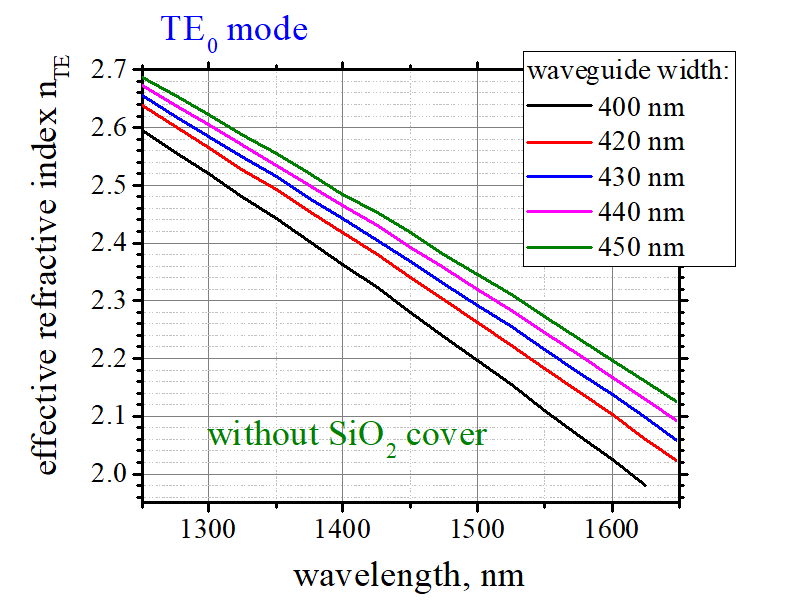
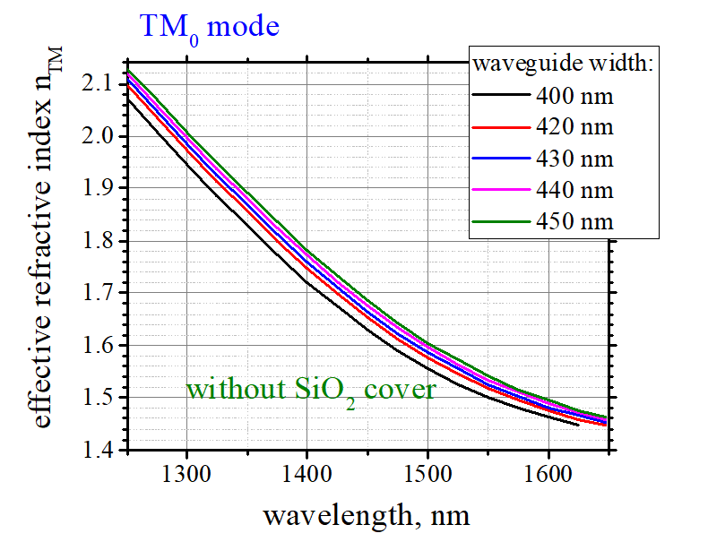
without SiO2cover |
||||||
|
||||||
| The refractive index is calculated by a conventional finite-difference method (see below) | ||||||
| The same data in text files nTEcoverWith.txt ; nTEcoverWithout.txt ; nTMcoverWith.txt ; nTMcoverWithout.txt | ||||||
| the same data in this free & open-source program (See here) | ||||||
| click on image to enlarge it |
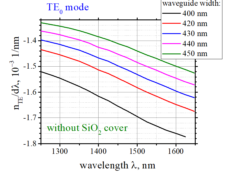
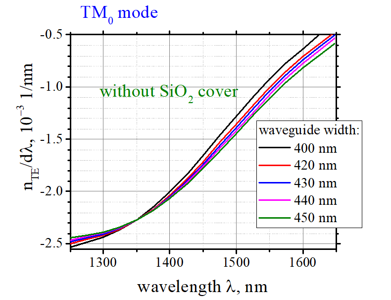
Dispersion dneff/dλ |
||||||
|---|---|---|---|---|---|---|
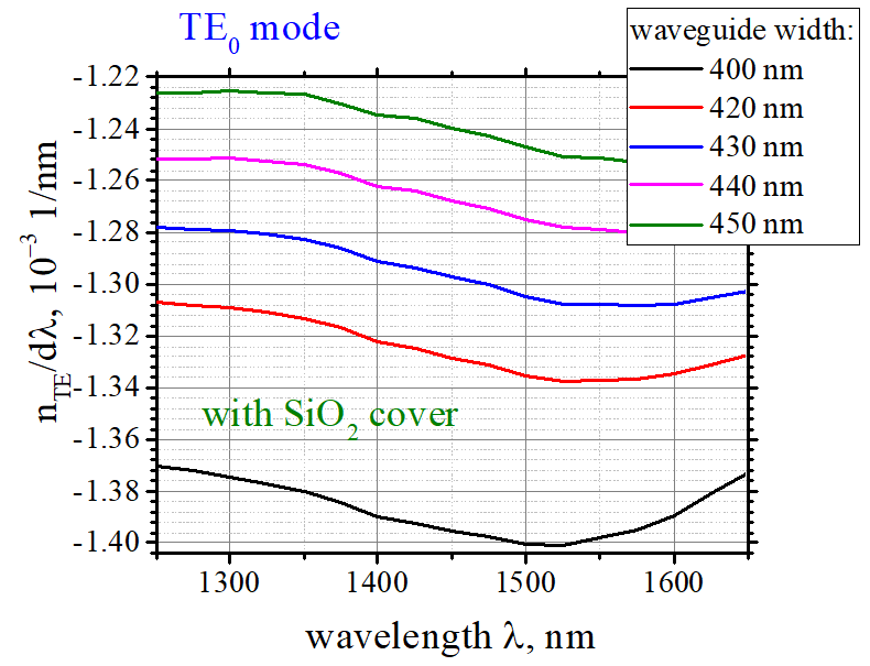
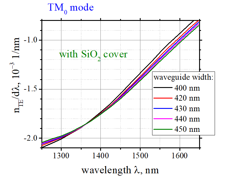
with SiO2 cover (cover thickness >1 μm) |
||||||
|
||||||
without SiO2cover |
||||||
|
||||||
| The refractive index is calculated by a conventional finite-difference method (see below) | ||||||
| The same data in text files dn_dl_TEcoverWith.txt ; dn_dl_TEcoverWithout.txt ; dn_dl_TMcoverWith.txt ; dn_dl_TMcoverWithout.txt | ||||||
| the same data in this free & open-source program (See here) | ||||||
| click on image to enlarge it |
 |
 |
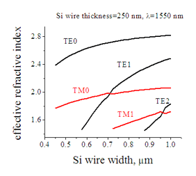 |
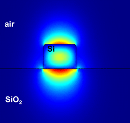
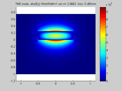
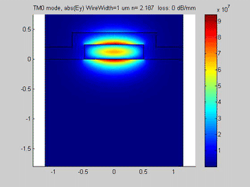
Fig.1 TM mode. Distribution of optical field in a Si wire waveguide width: 500 nm thickness 250 nm |
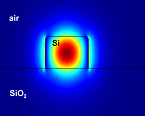
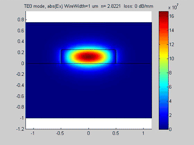
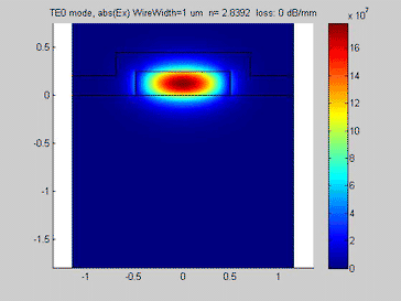
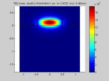
Fig. 2 TE mode. Distribution of optical field in a Si wire waveguide width:300 nm thickness 250 nm | Fig.3 Effective refractive index of waveguide modes in a 250-nm thick Si wire waveguide |
Optical field of TE mode is mainly inside the Si wire. Significant amount of optical field of TM mode is inside the SiO2 substrate.
 |
 |
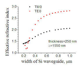 |
Fig.4 Animated picture. TM mode. Distribution of optical field in a Si wire waveguide Si thickness is 250 nm. Animated parameter is width of Si wire. |
Fig. 5. Animated picture. TE mode. Distribution of optical field in a Si wire waveguide. Si thickness is 250 nm. Animated parameter is width of Si wire. | Fig.6 Effective refractive index of waveguide modes in a 250-nm thick Si wire waveguide. The data is the same as shown in Fig.3. |
When Si waveguide width becomes narrow, the confinement of optical mode by the core layer becomes weak and eventually disappears.
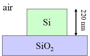
The 250 nm is an optimum thickness of Si on SiO2 for Si wire waveguide. For thicker Si the cutoff thicknesses for TE1 and TM1 modes becomes narrow (less than 500 nm) (See Fig. 3). In the case of a multimode waveguide, the devices performance are significantly limited. It is preferable to use a single-mode waveguides, which support only TE0 and TM0 modes. In the case of Si thickness thinner than 250 nm, the optical confinement for TM mode becomes weak. It is also undesirable for some applications.
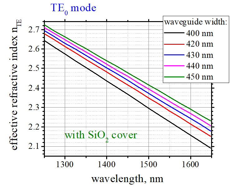
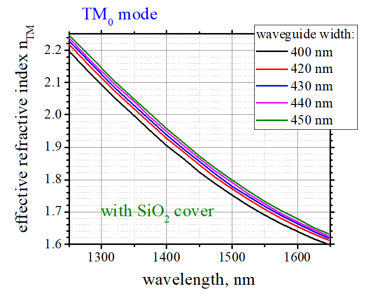
The cutoff width of 250-nm-wide Si-wire waveguide is about 250-350 nm (See Fig.6). The effective refractive index of TM0 and TE0 modes is about 1.7 and 2.7, respectively. The effective refractive index of TM0 mode is close to the refractive index of SiO2 (n=1.444) and the effective refractive index of TM0 mode is close to the refractive index of Si (n=3.48). That reflects the fact that the intensity of light for TM mode is mainly inside SiO2 (See Fig.4) and the intensity of light for TE mode is mainly inside Si (See Fig.5)
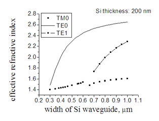
Comparing to 250-nm-thick Si wire, in case of Si thickness of 200 nm the properties of TE mode practically do not change. The effective refractive index of TE mode is about 2.6 (See Fig. 8). Therefore, TE mode is mainly inside Si. In contrast, TM mode is mainly inside SiO2 (See Fig.7). The effective refractive index of TM is very close to n of SiO2 (1.444) even in case of wide waveguides (~500 nm)
 |
 |
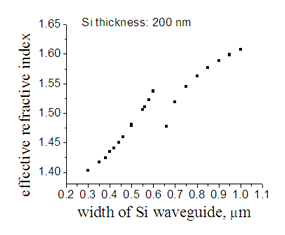 |
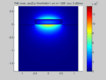
Fig.7 Animated picture. TM mode. Distribution of optical field in a Si wire waveguide. Si thickness is 200 nm. Animated parameter is width of Si wire. |
Fig.8 Effective refractive index of TM and TE waveguide modes in a 200-nm thick Si wire waveguide. | Fig.9 Effective refractive index of TM waveguide mode in a 200-nm thick Si wire waveguide. |
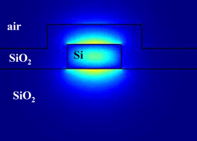 |
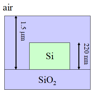
Fig.10 TM mode in Si wire waveguide covered by SiO2 |
In order to protect transition metals from oxidation the plasmonic waveguides need to be covered by a protection oxide. At the same time, the Si wire waveguides are covered as well. The covering of the Si wire waveguide by an oxide makes a little or no effect on TE mode, but it significantly influences the TM mode. The optical confinement of TM mode becomes more inside Si wire instead of SiO2 substrate. It is undesirable for efficient coupling with a plasmonic waveguide.
 |
 |
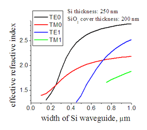 |
Fig.11 Animated picture. TM mode. Distribution of optical field in a Si wire waveguide covered by SiO2. Si thickness is 250 nm. SiO2 cover thickness is 200 nm. Animated parameter is width of Si wire. |
Fig.12 Animated picture. TE mode. Distribution of optical field in a Si wire waveguide covered by SiO2. Si thickness is 250 nm. SiO2 cover thickness is 200 nm. Animated parameter is width of Si wire. | Fig.12 Effective refractive index of waveguide modes in a 250-nm thick Si wire waveguide covered by 200 nm of SiO2. |
In this case the effective refractive index of TM mode is about 2, which is much higher than in the case without oxide. That means that the TM mode is significantly confined inside Si. Also, light significantly penetrates into the top SiO2 cover. This field distribution does not match field distribution of a surface plasmon. It is not good for efficient coupling between the waveguide mode and the plasmons.
 |
 |
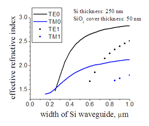 |
Fig.14 Animated picture. TM mode. Distribution of optical field in a Si wire waveguide covered by SiO2. Si thickness is 250 nm. SiO2 cover thickness is 50 nm. Animated parameter is width of Si wire. |
Fig.15 Animated picture. TE mode. Distribution of optical field in a Si wire waveguide covered by SiO2. Si thickness is 250 nm. SiO2 cover thickness is 50 nm. Animated parameter is width of Si wire. | Fig.16 Effective refractive index of waveguide modes in a 250-nm thick Si wire waveguide covered by 50 nm of SiO2. |
Comparing with 200 nm cover, the 50 nm cover is much better. It is more light inside SiO2 substrate. However, still the field distribution is not as good as in the case without SiO2 cover.
For calculations I have used Matlab or Matlab combined with Comsol Multiphysics
Files to download
*.m Matlab+ Comsol Files files
SiWaveguideModeWidth.m modes Si rib waveguide as function of rib width
WaveguideMode.m calculation of waveguide modes of rib waveguide (Comsol file: WaveguideMode.mph) used Geometry2D_Rib.m
AlGaAsWaveguide_Scan.m calculation of waveguide modes of rib AlGaAs waveguide. Scan of different parameters. File used RibWaveGeometry.m
comment about
The Si waveguides are used to delver light from/to an optical fiber to/from a plasmonic waveguide made on a Si substrate. TM mode near cutoff has similar optical field distribution as optical field distribution of the surface plasmons. Due to very high contrast in refractive index of Si wire waveguide, it is difficult (but possible) to match optical field of waveguide and plasmonic mode in the case of waveguide on Si. The optical field of TE mode is mainly inside Si core. In contrast, a significant amount of optical field of TM mode is inside SiO2. Therefore, it might be possible to achieve a sufficiently good matching between a wire waveguide and a plasmonic waveguide fabricated on Si