Dr. Vadym Zayets
v.zayets(at)gmail.com
My Research and Inventions
click here to see all content |

Dr. Vadym Zayetsv.zayets(at)gmail.com |
|
|
Surface Plasmons
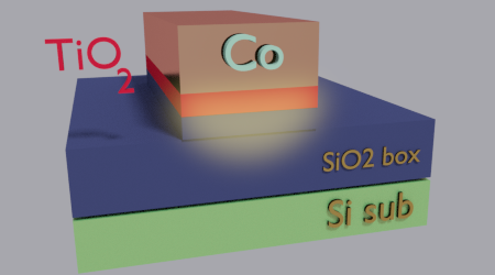
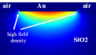
Metal-stripe plasmonic waveguide
There is a substantial scattering loss at the metallic edges of a plasmonic structure. To avoid this huge loss, the plasmon is confined at the center of the metallic structure. It push out the field of the plasmon from the edges of the metal and plasmonic loss is reduced. The bridge or grove or wedge is used for the in-plane confinement (See here).
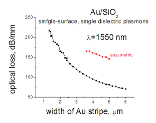
Au:SiO2 single-surface, single dielectric plasmons
The optical loss for plasmons in Au:SiO2 film is 45 dB/mm. It is smaller than in the Au:SiO2 stripe.
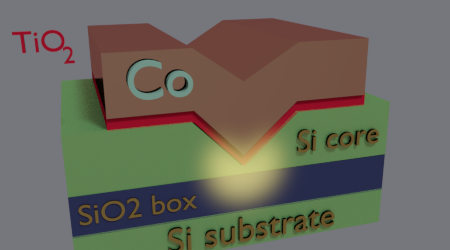
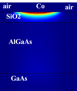
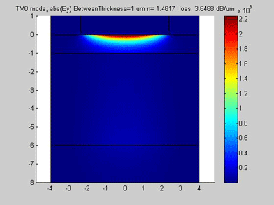
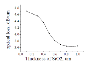
Co-SiO2-AlGaAs-GaAs plasmonic waveguide (lambda=800 nm)
The optical field is significantly confined inside SiO2 layer. There is no cutoff because of thickness of AlGaAs is not sufficient
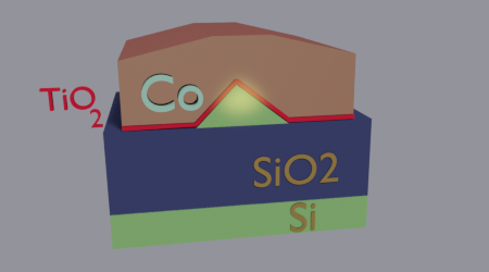
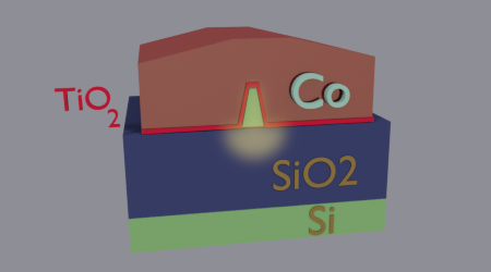
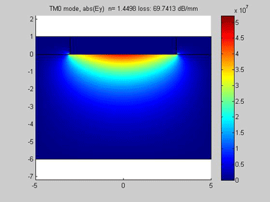
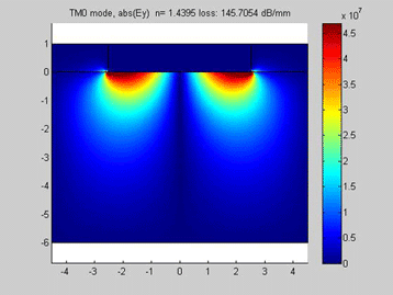
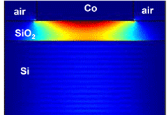
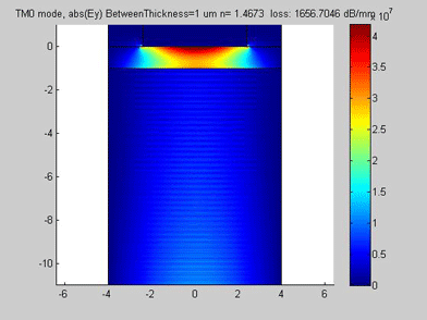
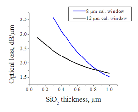
Co(strip)-SiO2-Si plasmonic waveguide (lambda=1550 nm)
There is a significant confinement of optical field inside SiO2 layer The calculated optical loss might be large than real value due to limitations of the calculation method (The dependence of calculated optical loss on the sizes of calculation window indicates the limitations of the calculation method). It is still a challenging task for me to calculate correctly the parameters of surface plasmons in a stripe-metal waveguide near cutoff by FEM method.
|
I will try to answer your questions as soon as possible