Dr. Vadym Zayets
v.zayets(at)gmail.com
My Research and Inventions
click here to see all content |

Dr. Vadym Zayetsv.zayets(at)gmail.com |
|
|
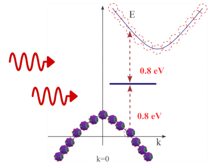
Two Photon Absorption in Si nanowire waveguide.
Si wire waveguidesThe two-photon absorption is a quantum process in which two photons are simultaneously absorbed, giving a valence-band electron enough energy to transition into the conduction band. This transition proceeds through a virtual state within the bandgap.page created in Dec. 2025
|
Two-electron absorption. The electron path |
|---|
|
| After |
| click on image to enlarge it |
Motivation
There are two main reasons.
![]() First, it is important to reduce unwanted nonlinear absorption, which limits the maximum data transmission capacity of silicon waveguides. Suppressing this effect would increase both the speed and the capacity of data transfer in silicon photonic circuits.
First, it is important to reduce unwanted nonlinear absorption, which limits the maximum data transmission capacity of silicon waveguides. Suppressing this effect would increase both the speed and the capacity of data transfer in silicon photonic circuits.
![]() Second, two-photon absorption itself can be exploited as a switching mechanism for all-optical data processing. If the strength of two-photon absorption could be controlled externally—for example, by applying a gate voltage to a silicon waveguide—it would enable ultrafast all-optical switching and, consequently, all-optical data processing based on this effect.
Second, two-photon absorption itself can be exploited as a switching mechanism for all-optical data processing. If the strength of two-photon absorption could be controlled externally—for example, by applying a gate voltage to a silicon waveguide—it would enable ultrafast all-optical switching and, consequently, all-optical data processing based on this effect.
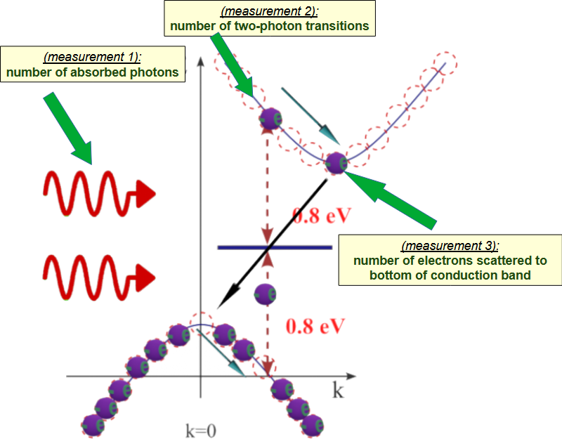
| There independent measurements to trace the dynamics of two- photon absorption |
|---|
 |
| click on image to enlarge it |
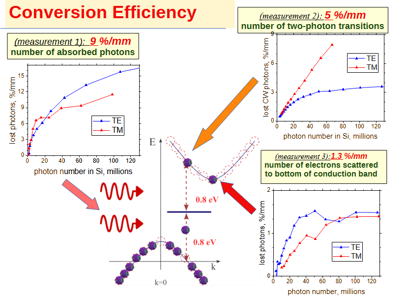
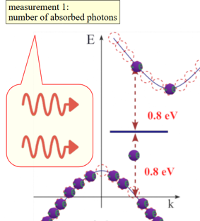
measurement 1: measurement of number of non-linearly absorbed photons |
|---|
|
| click on image to enlarge it |
![]() (What is measured?): Number of photon non-linearly absorbed in a nanowire Si waveguide
(What is measured?): Number of photon non-linearly absorbed in a nanowire Si waveguide
 (How is it measured?): Optical absorption is measured as a function of the pulse intensity in a nanowire Si waveguide
![]() (What is the goal of the measurement?): Comparing the number of nonlinearly absorbed photons with the number of photoexcited electrons (Measurement 2) can clarify whether two-photon absorption is the sole nonlinear optical process in a silicon nanowire waveguide or whether additional nonlinear effects are present.
(What is the goal of the measurement?): Comparing the number of nonlinearly absorbed photons with the number of photoexcited electrons (Measurement 2) can clarify whether two-photon absorption is the sole nonlinear optical process in a silicon nanowire waveguide or whether additional nonlinear effects are present.
 (Novelty): I proposed and demonstrated this measurement method for the first time.
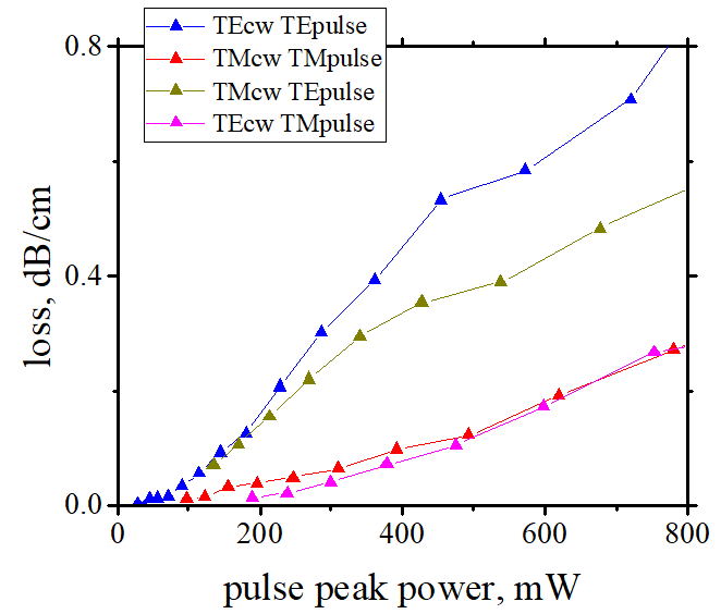
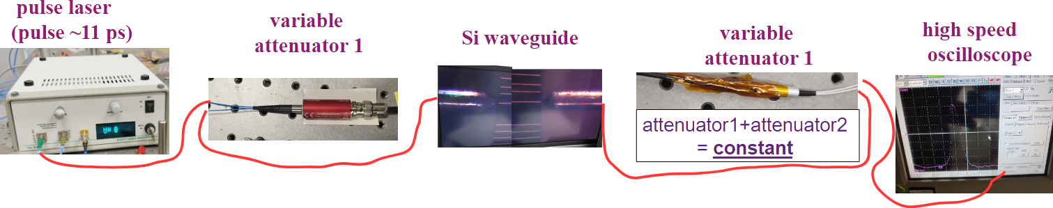
Setup for measurement 1: measurement of number of absorbed photons |
|---|
|
| A short optical pulse from a mode-locked laser, after passing through the first variable attenuator, is coupled into a silicon nanowire waveguide. After being coupled out from the waveguide, the pulse passes through a second variable attenuator before being measured by a high-speed oscilloscope. Both variable attenuators are computer-controlled to keep the total linear loss of the whole optical pulse till the oscilloscope unchanged while the pulse intensity inside the silicon waveguide is varied. |
| The key idea of this setup is the use of two synchronized variable attenuators. When the first attenuator increases, the second decreases proportionally, keeping the total attenuation constant. As a result, the pulse intensity entering the Si waveguide can be modulated, while the attenuation on the path to the oscilloscope is fixed. |
| click on image to enlarge it |
Raw measurement data. |
||||||||
|---|---|---|---|---|---|---|---|---|
|
||||||||
| With the silicon waveguide absent, varying the attenuators produces no change in the detected pulse, as the total linear loss is constant. This confirms the absence of nonlinear effects from the measurement components themselves, validating the setup. | ||||||||
| In contrast, when the Si waveguide is inserted, the detected pulse changes significantly. The nonlinear loss increases sharply with rising pulse intensity inside the Si waveguide. | ||||||||
| click on image to enlarge it |

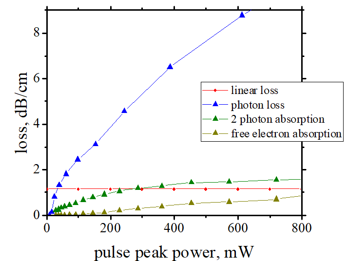
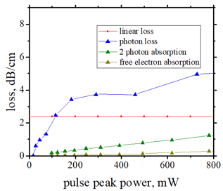
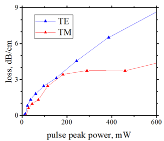
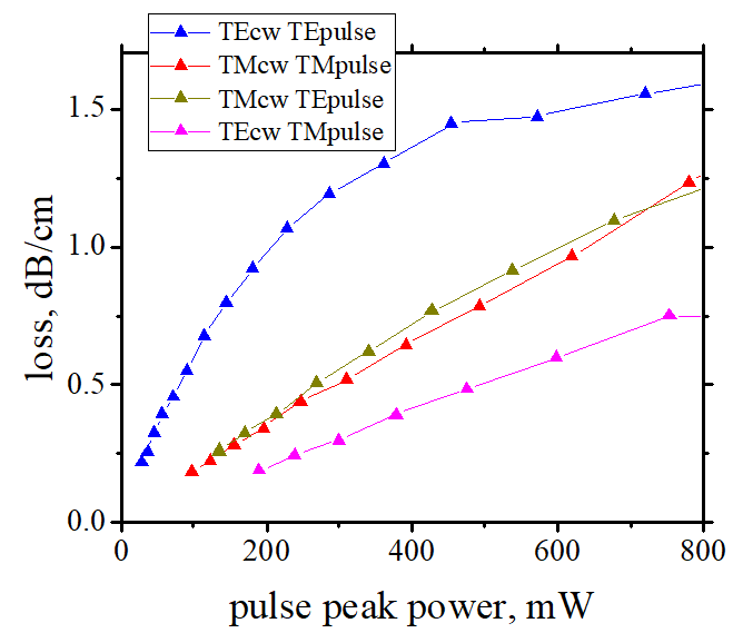
results. measurement 1: Optical loss |
||||||
|---|---|---|---|---|---|---|
|
||||||
| click on image to enlarge it |
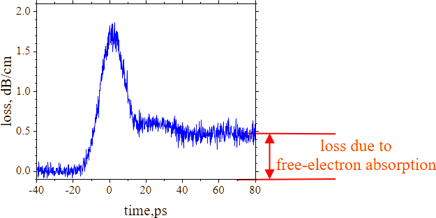
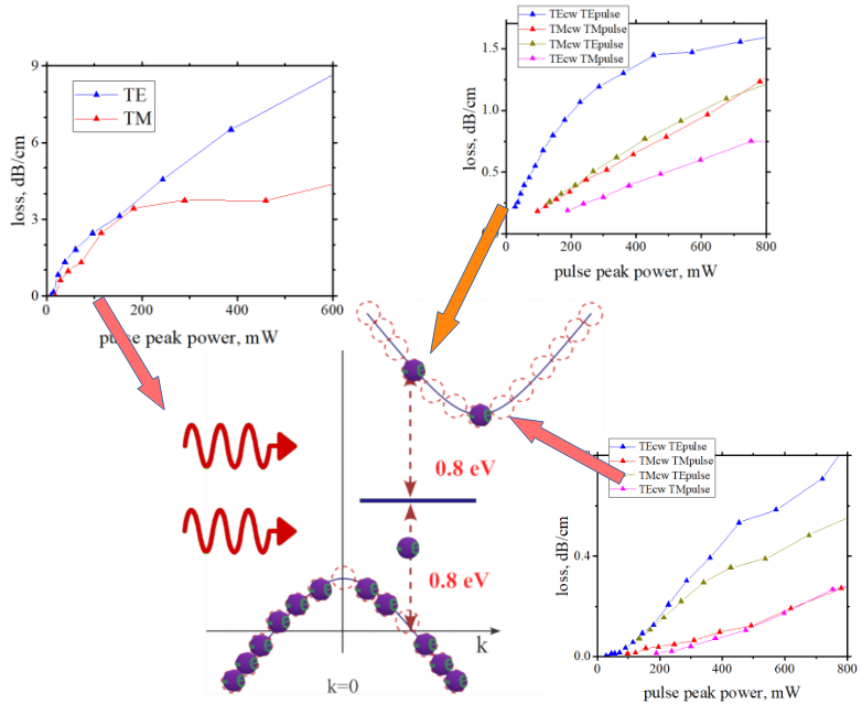
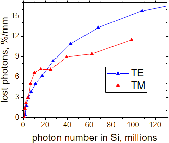
(fact): A key observation across all three measurement methods is that nonlinear loss for TM polarization is always substantially smaller than for TE polarization. This trend is opposite to that of linear loss: in our Si nanowire waveguides, the linear loss is about twice as large for TM as for TE.
![]() This type of nonlinear loss should be proportional to the square of the pulse intensity because:
This type of nonlinear loss should be proportional to the square of the pulse intensity because:
![]() each absorption event involves the simultaneous absorption of two photons from the optical pulse. Consequently, the photon loss scales with the square of the number of photons in the pulse, or equivalently, with the square of the pulse intensity.
each absorption event involves the simultaneous absorption of two photons from the optical pulse. Consequently, the photon loss scales with the square of the number of photons in the pulse, or equivalently, with the square of the pulse intensity.
![]() (point 1)
(point 1) ![]() Why is the nonlinear loss nearly the same for TE and TM modes at low power?
Why is the nonlinear loss nearly the same for TE and TM modes at low power?
Since the amount of optical power confined in silicon is approximately twice smaller for the TM mode than for the TE mode, the nonlinear loss for the TM mode should be roughly half that of the TE mode.
![]() (point 2)
(point 2) ![]() Why is the non-linear loss for TM mode saturated at a high power?
Why is the non-linear loss for TM mode saturated at a high power?
![]() (point 2)
(point 2) ![]() Why the shape of dependencies of the non-linear loss on pulse energy are so different for TE and TM modes?
Why the shape of dependencies of the non-linear loss on pulse energy are so different for TE and TM modes?
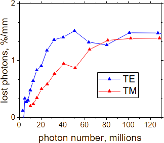
results. measurement 1: Loss of photons |
||||||
|---|---|---|---|---|---|---|
|
||||||
| The number of photons only inside the Si core is shown. The photons inside SiO2 are excluded. | ||||||
| (note) difference in distribution of TE and TM mode is taking into account (See here) |
 How was it calculated:
![]()
 Photon number is calculated as: (step 1) The pulse energy was calculated from the pulse peak intensity and the temporal pulse shape.; (step 2): The total number of photons in a single pulse was obtained by dividing the pulse energy by the photon energy. (step 3): The number of photons in the silicon core was calculated by multiplying the total photon number by the fraction of the optical mode power confined in the silicon core, which differs for TE and TM modes.
![]()
 Percentage of lost photons is calculated as: (step 1
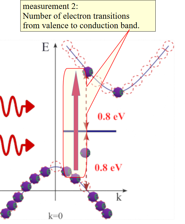
measurement 2: measurement of number of electron transitions from valence to conduction band due to two-photon absorption |
|---|
|
| click on image to enlarge it |
![]() (What is measured?): Number of two-photon transitions induced by optical pulse
(What is measured?): Number of two-photon transitions induced by optical pulse
![]()
![]() (Specific: What is measured?):Percentage of photons absorbed due to the two-photon absorption
(Specific: What is measured?):Percentage of photons absorbed due to the two-photon absorption
(How is it measured?): It measures the change of absorption of a weak CW light induced by a short optical pulse.
![]() (What is the goal of the measurement?): It is the most direct measurement of two-photon absorption. As a result, it gives most reliable measure of the efficiency of two-photon absorption.
(What is the goal of the measurement?): It is the most direct measurement of two-photon absorption. As a result, it gives most reliable measure of the efficiency of two-photon absorption.
 (Why is this measurement the most direct measurement of two-photon absorption?): This is because only a single physical mechanism can contribute to the measured signal: One photon from the continuous-wave (CW) light interacts with one photon from the optical pulse, inducing an electronic transition. Only this two-photon process can result in nonlinear absorption of the CW photon. Since the CW light intensity is low, it does not experience nonlinear effects on its own, thereby excluding contributions from all other possible nonlinear mechanisms.
 (Does this measurement provide the efficiency of two-photon absorption for the optical pulse?): Yes. It gives the probability that a single photon combines with any photon in the optical pulse to induce a two-photon electronic transition. This probability is universal for photons of the same energy of any original source and does not depend on whether the photon is from continuous-wave light, from an optical pulse, or from any other light source.
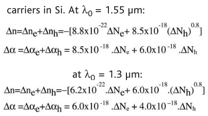
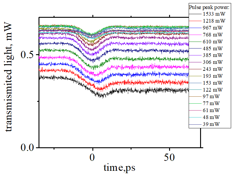
measurement 2:Transmission of CW probe vs. pulse peak power. Fig 14 |
|---|
|
| t=0 ps corresponds to arrival time of the pump pulse |
| (reduction of transmission before pulse arrival. negative time) Even before the arrival of the pump pulse the free-electron absorption still remains. It is because the free-electrons created by the free preceding pulse are not fully relaxed back to the valence band. As a result, CW transmission is reduced even before pulse arrival |
| (minimum peak): the shape of the minimum transmission corresponds to the shape of the pumping pulse. The reduction of transmission is due to two-photon absorption. |
| click on image to enlarge it |
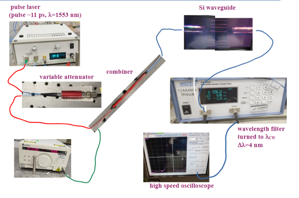
Setup for measurement 2:number of two-photon transitions.(same as measurement 3) |
|---|
|
| The outputs of the pulse laser and the CW laser, operating at slightly different wavelengths, are combined and coupled into the Si waveguide. After co-propagated through the silicon waveguide, the pulse is removed using a narrowband filter, so that only the CW light reaches the high-speed oscilloscope. In the presence of a pulse, the CW signal becomes modulated, enabling precise measurement of the nonlinear absorption dynamics. |
| (polarization switch): We independently controlled the polarization of both the pulsed and CW lasers, selecting either TE or TM mode for each. This allowed us to conduct measurements for all four possible combinations of input polarizations. |
| click on image to enlarge it |
Raw measurement data. |
||||||||
|---|---|---|---|---|---|---|---|---|
|
||||||||
| As you can see, the timing and shape of this loss match precisely with those of the modulation pulse. This confirms that the two-photon absorption of the CW light occurs only in the presence of the modulation pulse. | ||||||||
| Remaining loss after the completion of the two-photon absorption process is due to the free-electron absorption (see measurement 3) |
results. measurement 2: Optical loss |
||||||
|---|---|---|---|---|---|---|
|
||||||
| click on image to enlarge it |
![]() This type of nonlinear loss should be linearly proportional to of the pulse intensity because:
This type of nonlinear loss should be linearly proportional to of the pulse intensity because:
![]() Each absorption event involves the simultaneous absorption of one photon from the optical pulse and one photon from CW probe. Consequently, the loss of CW photons scales linearly with the number of photons in the pulse, or equivalently, linearly with the pulse intensity.
Each absorption event involves the simultaneous absorption of one photon from the optical pulse and one photon from CW probe. Consequently, the loss of CW photons scales linearly with the number of photons in the pulse, or equivalently, linearly with the pulse intensity.
In the classical picture, this loss should be linearly proportional to the pump pulse intensity, since one pump photon is absorbed together with one CW probe photon. Indeed, we observed this linear dependence for almost all pump/probe polarization combinations—except when both pump and probe were TE-polarized. In that case, the absorption saturates at peak powers above 300 mW. Moreover, classical theory predicts that TPA should occur only when the pump and probe have the same polarization. . In contrast, we observed comparable absorption for both co-polarized and cross-polarized configurations.
![]() Why is the peak position in fig 14 shifted with an increase of pulse power?
Why is the peak position in fig 14 shifted with an increase of pulse power?
results. measurement 2: Loss of photons |
||||||
|---|---|---|---|---|---|---|
|
||||||
| The number of photons only inside the Si core is only taken into account. The photons inside SiO2 are excluded. | ||||||
| (note) difference in distribution of TE and TM mode is taking into account (See here) |
How was it calculated:![]() Photon number is calculated as: (step 1) The pulse energy was calculated from the pulse peak intensity and the temporal pulse shape.; (step 2): The total number of photons in a single pulse was obtained by dividing the pulse energy by the photon energy. (step 3): The number of photons in the silicon core was calculated by multiplying the total photon number by the fraction of the optical mode power confined in the silicon core, which differs for TE and TM modes.
Photon number is calculated as: (step 1) The pulse energy was calculated from the pulse peak intensity and the temporal pulse shape.; (step 2): The total number of photons in a single pulse was obtained by dividing the pulse energy by the photon energy. (step 3): The number of photons in the silicon core was calculated by multiplying the total photon number by the fraction of the optical mode power confined in the silicon core, which differs for TE and TM modes.
![]() Percentage of lost photons is calculated as: (step 1) peak loss at moment of pump- pulse arrival is measured. (step 2) The rate of photon loss is calculated of this loss
Percentage of lost photons is calculated as: (step 1) peak loss at moment of pump- pulse arrival is measured. (step 2) The rate of photon loss is calculated of this loss
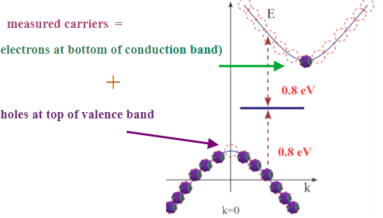
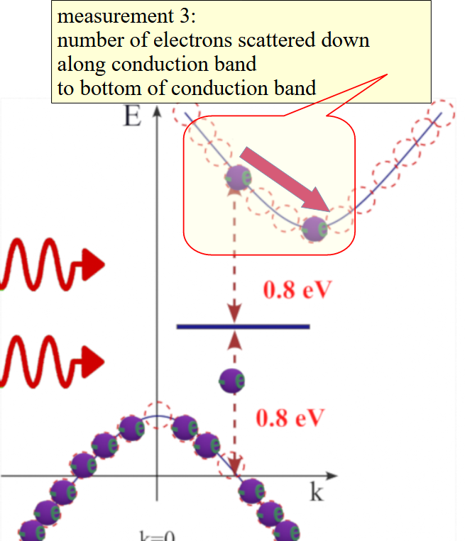
measurement 3: measurement of number of electrons scattered down along conduction band to bottom of conduction band plus number of holes scattered up along valence band to top of valence band |
|---|
|
| click on image to enlarge it |
![]() (What is measured?): After being excited from the valence band to the conduction band via the two-photon absorption mechanism, electrons rapidly scatter within the conduction band toward lower energies until they reach the bottom of the conduction band. Since the electronic transition from the conduction-band minimum to the valence-band maximum is indirect in silicon, the probability of such a transition is low. As a result, electrons remain near the bottom of the conduction band for a relatively long time (~70 ns) before recombining into the valence band. Measurement 3 quantifies the number of conduction electrons residing at the bottom of the conduction band that are generated by the two-photon absorption process.
(What is measured?): After being excited from the valence band to the conduction band via the two-photon absorption mechanism, electrons rapidly scatter within the conduction band toward lower energies until they reach the bottom of the conduction band. Since the electronic transition from the conduction-band minimum to the valence-band maximum is indirect in silicon, the probability of such a transition is low. As a result, electrons remain near the bottom of the conduction band for a relatively long time (~70 ns) before recombining into the valence band. Measurement 3 quantifies the number of conduction electrons residing at the bottom of the conduction band that are generated by the two-photon absorption process.
![]()
![]() (Specific: What is measured?): The number of free-electrons measured from optical absorption of CW probe immidietly after the probe pulsed passed the Si waveguide. Free-electron absorption is measured in the time interval immediately following the completion of the two-photon absorption process. The silicon nanowire waveguide is fabricated from semi-insulating silicon and therefore contains no free carriers under equilibrium conditions. All free electrons detected in this measurement are generated by the two-photon absorption process.
(Specific: What is measured?): The number of free-electrons measured from optical absorption of CW probe immidietly after the probe pulsed passed the Si waveguide. Free-electron absorption is measured in the time interval immediately following the completion of the two-photon absorption process. The silicon nanowire waveguide is fabricated from semi-insulating silicon and therefore contains no free carriers under equilibrium conditions. All free electrons detected in this measurement are generated by the two-photon absorption process.
(How is the number of free electrons measured from optical absorption?): The optical absorption caused by free electrons and free holes in silicon is well calibrated in measurement of Si optical modulator. These data are critical and are widely used in the design and optimization of silicon optical modulators. Therefore, by measuring the free-carrier–induced optical absorption, the corresponding density of free electrons (and holes) can be quantitatively determined.
![]() (What is the goal of the measurement?): The goal is to determine whether all electrons excited via the two-photon absorption mechanism are scattered to the bottom of the conduction band, or whether alternative pathways exist that allow excited electrons to return to the valence band without reaching the conduction-band minimum.
(What is the goal of the measurement?): The goal is to determine whether all electrons excited via the two-photon absorption mechanism are scattered to the bottom of the conduction band, or whether alternative pathways exist that allow excited electrons to return to the valence band without reaching the conduction-band minimum.
|
|---|
|
| change of refractive index and absorption vs. free carrier |
| data from calibration of Si optical modulator modulator |
| Since numbers of excited holes and electrons, their number is calculated from the measured free- carrier optical absorption. |
Setup for measurement 3:number of electrons scattered to bottom of conduction band(same as measurement 3) |
|---|
|
| The outputs of the pulse laser and the CW laser, operating at slightly different wavelengths, are combined and coupled into the Si waveguide. After co-propagated through the silicon waveguide, the pulse is removed using a narrowband filter, so that only the CW light reaches the high-speed oscilloscope. In the presence of a pulse, the CW signal becomes modulated, enabling precise measurement of the nonlinear absorption dynamics. |
| (polarization switch): We independently controlled the polarization of both the pulsed and CW lasers, selecting either TE or TM mode for each. This allowed us to conduct measurements for all four possible combinations of input polarizations. |
| click on image to enlarge it |
Raw measurement data. |
||||||
|---|---|---|---|---|---|---|
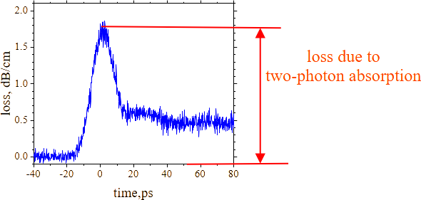
Temporal evolution of optical loss for CW probe. |
||||||
|
||||||
| Time-resolved optical loss of CW probe measured by high-speed optical oscilloscope. TE mode. pulse peak power 477 mW | ||||||
| The free-electron absorption is measured as the step height of CW absorption before and after the modulation pulse. This residual absorption is caused by free carriers (electrons and holes) generated by the pulse. The pulse generates equal numbers of free electrons and holes, |
 |
|
results. measurement 3: Optical loss |
||||||
|---|---|---|---|---|---|---|
|
||||||
| click on image to enlarge it |
![]() This type of nonlinear loss should be proportional to the square of the pulse intensity because:
This type of nonlinear loss should be proportional to the square of the pulse intensity because:
![]() the free-carrier absorption is directly proportional to the number of electrons in the conduction band. The number of conduction electrons is proportional to the number of two-photon absorption events, which in turn scales with the square of the number of photons in the pulse, or equivalently, with the square of the pulse intensity.
the free-carrier absorption is directly proportional to the number of electrons in the conduction band. The number of conduction electrons is proportional to the number of two-photon absorption events, which in turn scales with the square of the number of photons in the pulse, or equivalently, with the square of the pulse intensity.
Since creating an electron-hole pair requires the simultaneous absorption of two photons from the pump pulse, the classical model predicts this loss should be proportional to the square of the pump intensity. Our measurements confirm this only at low powers (< 100 mW). At higher powers, the dependence becomes linear. Also, because the free carriers are generated solely by the pump pulse—not the CW probe—the measured loss should be independent of probe polarization. This trend is indeed observed experimentally.
results. measurement 3: Loss of photons |
||||||
|---|---|---|---|---|---|---|
|
||||||
| The number of photons only inside the Si core is only taken into account. The photons inside SiO2 are excluded. | ||||||
| (note) difference in distribution of TE and TM mode is taking into account (See here) |
How was it calculated:![]() Photon number is calculated as: (step 1) The pulse energy was calculated from the pulse peak intensity and the temporal pulse shape.; (step 2): The total number of photons in a single pulse was obtained by dividing the pulse energy by the photon energy. (step 3): The number of photons in the silicon core was calculated by multiplying the total photon number by the fraction of the optical mode power confined in the silicon core, which differs for TE and TM modes.
Photon number is calculated as: (step 1) The pulse energy was calculated from the pulse peak intensity and the temporal pulse shape.; (step 2): The total number of photons in a single pulse was obtained by dividing the pulse energy by the photon energy. (step 3): The number of photons in the silicon core was calculated by multiplying the total photon number by the fraction of the optical mode power confined in the silicon core, which differs for TE and TM modes.
![]() Percentage of lost photons is calculated as: (step 1) From the change in transmission of the CW probe light before and after the passage of the pump pulse, the optical loss due to free-carrier absorption was calculated. (step 2) Using calibrated free-carrier absorption data, the corresponding number of free electrons and holes was calculated from the measured free-carrier absorption. (step 3) The number of lost photons was then obtained as the number of photons required to generate the measured number of free electrons and holes by two-photon- absorption mechanism.
Percentage of lost photons is calculated as: (step 1) From the change in transmission of the CW probe light before and after the passage of the pump pulse, the optical loss due to free-carrier absorption was calculated. (step 2) Using calibrated free-carrier absorption data, the corresponding number of free electrons and holes was calculated from the measured free-carrier absorption. (step 3) The number of lost photons was then obtained as the number of photons required to generate the measured number of free electrons and holes by two-photon- absorption mechanism.
Two-electron absorption. The electron path |
|---|
|
| After |
| click on image to enlarge it |
 Comparison of Non- linear and Linear Optical losses. Limitation for Si Photonics
![]() (fact 1): non-linear loss is substantially larger than linear loss even for small power (~100 mW)
(fact 1): non-linear loss is substantially larger than linear loss even for small power (~100 mW)
![]() (fact ) for TM is twice larger than for TE
(fact ) for TM is twice larger than for TE
| Comparison of Non- linear and Linear Optical losses | ||||||
|---|---|---|---|---|---|---|
|
||||||
| Linear (red line) and Non- linear (blue and green lines) absorptions in a Si nanowire waveguide | ||||||
| q | ||||||
| click on image to enlarge it |
![]()

![]() (key observation) The first key observation is that non-linear losses are significantly larger than linear loss, even at relatively small peak powers (~100 mW). Given its magnitude, nonlinear loss must be a critical consideration in the design of high-speed photonic circuits.
(key observation) The first key observation is that non-linear losses are significantly larger than linear loss, even at relatively small peak powers (~100 mW). Given its magnitude, nonlinear loss must be a critical consideration in the design of high-speed photonic circuits.
 (possible solution of a problem for ultra- high-speed Si Photonic Circuits): If nonlinear loss becomes a limiting factor, one potential solution is to switch the operating mode from TE to TM. As the graph shows, nonlinear loss is significantly smaller for the TM mode, becoming comparable to the linear loss level. Currently, most photonic circuits are designed for TE mode only, but this choice may need to be reconsidered.
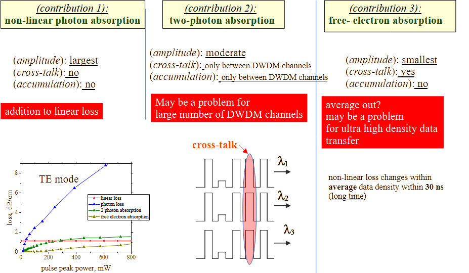
Although their magnitudes differ, each type of the three types of non-linear loss affects transmission in a distinct way:
 Bad effect of non-linear loss for high-speed Si photonics:
Nonlinear loss may impose a significant limitation on the speed of high-speed silicon photonic systems. It can introduce crosstalk between different channels as well as between preceding and subsequent pulses, thereby degrading the signal-to-noise ratio. Nonlinear loss also increases overall optical attenuation, which may reduce the signal below the detection threshold. Furthermore, these losses can accumulate, particularly at higher data transmission rates, leading to additional performance degradation.
| Non- linear Optical loss: limitation for Si Photonics |
|---|
 |
| click on image to enlarge it |
 (non-linear loss 1): photon loss
Intrinsic non-linear pulse loss is the largest. However, it behaves similarly to linear loss—it does not accumulate or cause cross-talk. It only becomes problematic in very long Si waveguides or when pulses of different amplitudes are transmitted.
(non-linear loss 2): Two-photon absorption loss
Two-photon absorption loss is smaller, but more critical in dense wavelength-division multiplexing systems. Since two-photon absorption occurs only during the pulse, pulses from different DWDM channels that are temporally aligned can experience significant cross-talk.
(non-linear loss 3): Free-carrier absorption loss
Free-carrier absorption loss is the smallest, but it accumulates over relatively long timescales. While averaging can mitigate this effect, this loss may still cause problems when average transmission is not constant but varies slowly with time. Despite its magnitude, this loss is instantaneous and does not accumulate. It behaves similarly to linear loss in that it does not cause crosstalk. It becomes problematic only when waveguides are very long or when using pulses with significantly different amplitudes, as it can distort the signal shape.
 |
| click on image to enlarge it |
| Conversion efficiency of photons to photo-excited electrons in conduction band |
|---|
 |
| click on image to enlarge it |
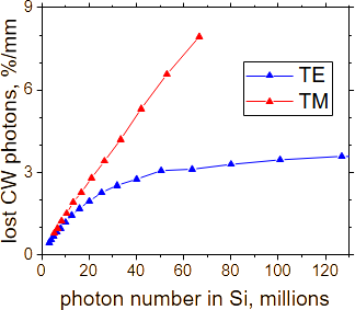
The conversion efficiencies obtained from all three methods are clearly not identical. The largest conversion efficiency is observed for intrinsic non-linear pulse absorption. A moderate efficiency is found for two-photon absorption. The smallest efficiency is associated with free-carrier absorption. Both the polarization dependence and the functional dependence on photon number distinctly differ across the three measurements.
![]()
![]() (Observation 1) :The number of photons absorbed in the silicon waveguide is larger—approximately twice—the number of two-photon transitions. This indicates that two-photon absorption is not the only nonlinear optical process present and that additional nonlinear loss mechanisms contribute in the silicon waveguide.
(Observation 1) :The number of photons absorbed in the silicon waveguide is larger—approximately twice—the number of two-photon transitions. This indicates that two-photon absorption is not the only nonlinear optical process present and that additional nonlinear loss mechanisms contribute in the silicon waveguide.
![]()
![]() (Observation 2) :The efficiency of two-photon absorption saturates much more rapidly for the TE mode than for the TM mode. In contrast, the saturation behavior of the total nonlinear photon absorption shows only slight difference between TE and TM polarizations.
(Observation 2) :The efficiency of two-photon absorption saturates much more rapidly for the TE mode than for the TM mode. In contrast, the saturation behavior of the total nonlinear photon absorption shows only slight difference between TE and TM polarizations.
![]()
![]() (Observation 3) :The number of two-photon transitions is significantly larger than the number of free carriers generated by these transitions. This implies the existence of additional relaxation pathways for photoexcited electrons from the conduction band back to the valence band, beyond the indirect phonon-assisted recombination from the conduction-band minimum to the valence-band maximum.
(Observation 3) :The number of two-photon transitions is significantly larger than the number of free carriers generated by these transitions. This implies the existence of additional relaxation pathways for photoexcited electrons from the conduction band back to the valence band, beyond the indirect phonon-assisted recombination from the conduction-band minimum to the valence-band maximum.
![]()
![]() (Observation 4) :The free-carrier density saturates at nearly the same photon number for both TE and TM modes. This behavior contrasts with the strong polarization dependence observed for the efficiency of two-photon transitions.
(Observation 4) :The free-carrier density saturates at nearly the same photon number for both TE and TM modes. This behavior contrasts with the strong polarization dependence observed for the efficiency of two-photon transitions.
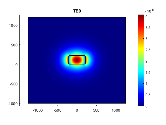
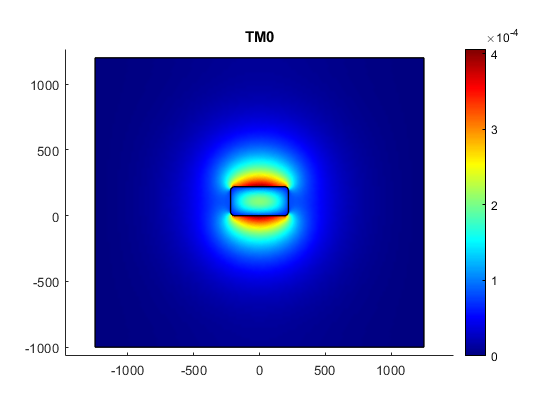
(fact):TE mode is strongly confined within the silicon core. In contrast, a significant portion of the TM mode's field resides in the surrounding SiO₂ cladding. TM mode has nearly half its field in SiO₂.
Different field distribution of TE and TM modes. Near- field measurements |
||
|---|---|---|
 |
||
| Near- field measurements. Experiementaly measured near-field distribution for TE and TM modes in Si nanowire waveguide | ||
|
||
| calculatednear-field distribution for TE and TM modes in Si nanowire waveguide | ||
| In both cases, it is evident that the TE mode is strongly confined within the silicon core. In contrast, a significant portion of the TM mode's field resides in the surrounding SiO₂ cladding. TM mode has nearly half its field in SiO₂. |
Since two-photon absorption occurs only in Si, not in SiO₂, the nonlinear absorption is stronger for TE than TM, consistent with our observations.
When we took into account the field distribution differences, we found that he polarization dependence of nonlinear absorption still exists, but becomes less prominent
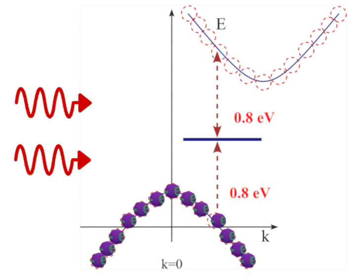
There are two possible mechanisms, which forms a middle gap levels in semiconductor:
![]() (middle-gap level type 1): bulk type
(middle-gap level type 1): bulk type
In the middle of the bandgap of a semiconductor, electrons can occupy quantum states that are not stable stable quantuum state or even not- existed quantum states in the usual sense. For this reason, mid-gap states are commonly referred to as virtual states. The true physical nature of these mid-gap states in the bulk of a semiconductor is still not fully understood.
![]() (middle-gap level type 2): surface type
(middle-gap level type 2): surface type
The surface states exist due to breaking of periodicity of semiconductor lattice and a boundary of the semiconductor. In contrast to virtual states in the bulk of a semiconductor, surface states are conventional, stable quantum states, similar to the quantum states in the conduction and valence bands.
Mechanisms of non-linear absorption(mechanism/origin 1) ![]() ?????
?????![]() ?????
?????![]() ?????
?????![]() ?????
?????![]() ?????
?????![]() ?????
?????![]()
 ???
??? ???(Possible origins 1) of non-linear loss & mid-gap "virtual" level: quantuum state , which energy has a complex part.
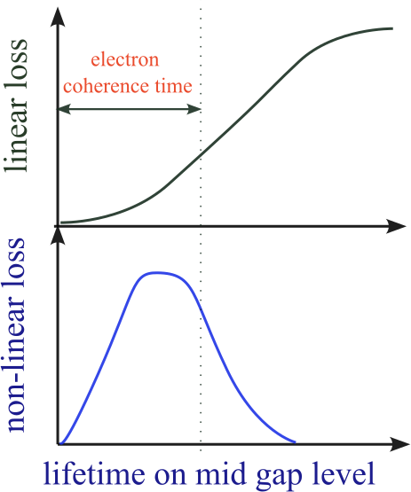
Dependence of linear and non-linear loss on lifetime on mid gap level |
|---|
|
| (linear loss) In the case of a short lifetime of midgap level, the electron after being excited to the level immediately returns back to its initial state in the valence band emitting a photon fully coherent to the absorbed photon. As a result, the number of photons in the pulse remains unchanged and there is no linear loss. In the case of a long lifetime the emitted photon is non- coherent and there is a linear loss. |
| (non-linear loss) An electron excited to a mid-gap level contributes to nonlinear loss only if it is subsequently excited to the conduction band and only if it does not contribute to linear optical loss. In the case of a short lifetime of midgap level, the probability for the electron to interact with a second photon to be exited from mid-gap to the conduction band is very small. In the case of a long lifetime the electron excited to the mid-gap contributes only to the linear loss, but not to the non-linear loss. |
| click on image to enlarge it |
![]() (fact) A mid-bandgap energy level with a very short lifetime does not cause linear optical loss but gives rise to nonlinear loss
(fact) A mid-bandgap energy level with a very short lifetime does not cause linear optical loss but gives rise to nonlinear loss
![]() (reason): why a short-lifetime level does not produce linear optical loss
(reason): why a short-lifetime level does not produce linear optical loss
When an electron is excited to a short-lived mid-gap state by a photon, it returns almost immediately to its initial state in the valence band, emitting a photon that is coherent with (i.e., identical to) the photon , which initially excited the electron (the simulating emission). Because the photon is re-emitted with the same energy and phase and in the same direction, the net number of photons is unchanged, and no linear optical loss occurs.
![]() (reason): why a short-lifetime level leads to nonlinearity
(reason): why a short-lifetime level leads to nonlinearity
Immediately after being excited to the middle level by the first photon, the electron interacts with a second photon. As a result, the electron is excited to the conduction band. The carrier lifetime in the conduction band is much longer, so there is no emission of a coherent photon. Therefore, photons are effectively removed from the optical field, producing nonlinear absorption. Since this process requires two photons, it manifests as a nonlinear optical effect.
![]() (reason): why the energy of a mid-gap state has a complex part
(reason): why the energy of a mid-gap state has a complex part
(Brag reflection for electron)
(similarity with complex refractive index)
(a specific solution of Dirac or Schrodinger equation)
![]()
![]()
![]() (argument against)
(argument against)
-------
(mechanism/origin 2) ![]() ?????
?????![]() ?????
?????![]() ?????
?????![]() ?????
?????![]() ?????
?????![]() ?????
?????![]()
??????(Possible origins 2) of non-linear loss & mid-gap "virtual" level:: Modification of the band structure due to interaction with many photons
Similar to how a strong static electric field applied to an atom can shift and modify atomic energy levels (Stark effect), a strong oscillating optical field can modify the electronic energy structure in a semiconductor. The combined optical field of many photons can induce quantum states within the bandgap, which are often called field-dressed (or light-field dressed) dynamic states. Electrons from the valence band can be excited into these states, leading to photon loss and thus nonlinear absorption. As the amplitude of the optical field increases, the field-induced modification of the electronic states becomes stronger, the density of these states becomes larger and the probability of such transitions correspondingly increases.
![]() (reason): why oscillating optical field creates the mid-gap level:
(reason): why oscillating optical field creates the mid-gap level:
The bandgap in a crystal arises from the periodic potential of the atomic lattice and the resulting Bragg reflection of electron waves. A strong oscillating optical field perturbs this periodic potential. Since the perfect periodicity is broken, the oscillating optical field can modify the band structure and enable quantum states within the bandgap.
![]()
![]()
![]() (argument against)
(argument against)
A very large electrical field is required to modify the band structure of solid. It is unclear whether the pulse power, which was used in our measurements, is sufficient for a such modification
![]()
 (effect on non-linear photon absorption):
(effect 1): dependency of photon loss vs photon number should be linear with saturation.
Since
(effect 2): It should be polarization independent. It should be equal for any combinations of polarizations of probe and pump
(mechanism/origin 3) ![]() ?????
?????![]() ?????
?????![]() ?????
?????![]() ?????
?????![]() ?????
?????![]() ?????
?????![]()
??????(Possible origins 3) of non-linear loss: three particle interaction (photon+photon +electron)
This corresponds to a process in which a single electron interacts simultaneously with two photons and absorbs the combined energy of both.
![]()
![]()
![]() (argument against)
(argument against)
Simultaneous interaction of 3 elementary particles is rarely observed in nature.
Contrargument: well- known and rather- strong 3 particle interaction interaction of a photon, phonon and electron: the indirect optical transition
![]() (effect on non-linear photon absorption):
(effect on non-linear photon absorption):
(effect 1): dependency of photon loss vs photon number should be linear with no saturation.![]()
Since it is the three- particle interaction, the surrounding environment should not influence this process and the type of dependency should not change with an increased number of photons
(effect 2): This mechanism should exist only for the photon of the same polarization and should not exist for cross-polarized photons
(mechanism/origin 4) ![]() ?????
????? ![]() ?????
????? ![]() ?????
????? ![]() ?????
?????![]() ?????
?????![]() ?????
?????![]()
??????(Possible origins 4 of non-linear loss: modification of coherence time for holes
As the light intensity increases, the number of electrons excited from the valence band to the mid-gap level increases, and the corresponding number of holes in the valence band also increases. Interactions among these holes reduce their coherence time, which in turn enhances nonlinear optical loss.
The nonlinear optical loss depends on the coherence time of the holes for the following reason. After excitation to the mid-gap level, an electron may return to its initial state in the valence band, emitting a photon. If this back-transition occurs rapidly and the coherence of the initial valence-band state is preserved, the emitted photon has the same phase and propagation direction as the initially absorbed photon. In this case, the total number of photons in the optical pulse remains unchanged, and no optical loss occurs.
In contrast, if the back-transition occurs after the coherence of the initial state has been degraded, the emitted photon is no longer coherent with the optical pulse. As a result, the photon is effectively removed from the optical field, leading to optical loss.
![]() (effect on non-linear photon absorption):
(effect on non-linear photon absorption):
(effect 1): dependency of photon loss vs photon number should be linear with no saturation.![]()
Since it is the three- particle interaction, the surrounding environment should not influence this process and the type of dependency should not change with an increased number of photons
-
![]() (comment from Andrej (mathematician)): The virtual state is a mathematical tool, but not a real thing with a physical meaning
(comment from Andrej (mathematician)): The virtual state is a mathematical tool, but not a real thing with a physical meaning
![]()
 (dependency 1): linear with no saturation:
 ![]() , where a is independent of N
, where a is independent of N
(possibility 1) three-prticle interaction (photon-photon-electron interaction in absence of mid-gap level)
This is the case of only three particle interaction (photon+photon +electron), when the non-linear absorption does not saturate at any pulse intensity. All other mechanisms do saturate. However, the saturated intensity might be very high and non- achievable in experimental measurements.
(possibility 2) three-prticle interaction (photon-photon-electron interaction in absence of mid-gap level)
This
![]() (dependency 2): linear with saturation:
(dependency 2): linear with saturation: ![]()
There are two cases when the non-linear absorption may saturate. See below.
![]() (dependency 3): constant:
(dependency 3): constant: ![]()
It is similar to linear loss. However, it is non-linear loss saturated at some specific pulse intensity
The saturation may occur due to a finite density of state for the mid- bandgap level.
(possibility 1) saturation of density of states for mid- bandgap level created by combined oscillating electrical field of all photons
At low and moderate photon numbers, the density of states associated with a field-induced mid-bandgap level may be approximately proportional to the optical field strength (or photon number). However, at higher photon numbers, the modification of the band structure does not lead to further increase in the density of states. That saturates the non-linear absorption.
(possibility 2) Saturation due to limited density of state , which energy has a complex part. Saturation when all electrons, which are excited to mid- bandgap level, are excited further to the conduction band.
At low and moderate photon numbers, some of the electrons excited to mid- bandgap level may return back to the valence band. However, at higher photon numbers, all electrons, which are excited to mid- bandgap level, are excited further to the conduction band. That saturates the non-linear absorption.
(path 1) :![]() emitting a second-harmonic photon.
emitting a second-harmonic photon.
emmiting of 2nd harmonic photon |
|---|
|
| After an electron undergoes a transition from the valence band to the conduction band via two-photon absorption, it can subsequently relax back to the valence band, emitting a second-harmonic photon. The energy of the emitted photon equals the sum of the energies of the two absorbed photons. |
| click on image to enlarge it |
(path 2) :![]() emitting photons at energies different from that of absorbed photons
emitting photons at energies different from that of absorbed photons
emitting photons at energies different from that of absorbed photons |
|---|
|
| After |
| click on image to enlarge it |
 (about lifetime on middle-bandgap level)
![]() (Mark's thoughts)
(Mark's thoughts)
(instantaneous lifetime due to Heisenberg uncertainty principle )
the lifetime of the virtual level in two photon absorption (TPA) is essentially instantaneous and limited by the Heisenberg uncertainty principle. Measurement evidence was also found in this paper ![]() describing the autocorrelation measurement of ~7fs pulses by TPA, which if its virtual state lifetime was longer then 7fs, then that would have limited the autocorrelation measurement resolution to > 7 fs so it seems cased closed on that question.
describing the autocorrelation measurement of ~7fs pulses by TPA, which if its virtual state lifetime was longer then 7fs, then that would have limited the autocorrelation measurement resolution to > 7 fs so it seems cased closed on that question.
(Heisenberg uncertainty principle vs. separation between two photons)
My interpretation was that the virtual energy level in two photon absorption (TPA) is just that-virtual only and the two photons need to be at the same place at the same time, and the precision of defining the position of the electron that can absorb those two photons is limited by the Heisenberg uncertainty principle, which sounds reasonable. On the other hand, if considering their wavefunctions, then I agree, TPA is still possible for even widely separated photons in space however, the probability would be far less. The autocorrelation measurement of ultra short pulses using TPA is a convincing way of showing that the lifetime of the virtual energy level is mostly instantaneous (by determining the minimum temporal resolution of the material), at least in that material, and the low probability of TPA for more widely separated photons is background noise.
As you pointed out, Heisenberg’s uncertainty principle was referring to the uncertainty of the electron’s spatial position (distance) in space, not time, and the lifetime of the virtual energy level in TPA is interpreted as the time it takes for the photon to traverse that distance (spatial location where the electron exists), limited by the Heisenberg uncertainty principle for defining the electron’s position in space. Nevertheless, I agree much longer lifetimes are still possible as determined by the overlapping wavefunctions, although with much less probability.
![]() (my thoughts)
(my thoughts)
(two-photon absorption used for autocorrelation)
Yes, two-photon absorption (TPA) is often used for autocorrelation of short optical pulses, which is commonly interpreted as evidence that the lifetime of the mid-gap (virtual) state is short. However, reported values for this lifetime are quite controversial, ranging from a few femtoseconds up to nearly 1000 fs (~1 ps).
I do not think that this lifetime is fundamentally fixed by the Heisenberg uncertainty principle. In my view, the uncertainty principle does not play a key role in TPA and may not influence it at all.
![]() (Role of the Heisenberg uncertainty principle)
(Role of the Heisenberg uncertainty principle)
The Heisenberg uncertainty principle applies to processes in which energy is not conserved. This is not the case for TPA: in two-photon absorption, energy is fully conserved—the combined energy of the two absorbed photons equals the energy gained by the excited electron.
![]() (example 1): (where the Heisenberg uncertainty principle works): dark matter / vacuum fluctuations.:
(example 1): (where the Heisenberg uncertainty principle works): dark matter / vacuum fluctuations.:
An electron–positron pair can be created from the vacuum state even though the energy of the electron- positron pair is larger than the vacuum energy.. This breaking of the energy conservation is allowed only for a very short time due to the Heisenberg uncertainty principle.
![]() (example 2): (where the Heisenberg uncertainty principle works): magnetic moment of the ground state:
(example 2): (where the Heisenberg uncertainty principle works): magnetic moment of the ground state:
If the ground state has no spin or orbital magnetic moment, but an excited state does, the ground state can still acquire a small magnetic moment. This occurs because the electron briefly occupies the excited state without an external energy source. Again, energy conservation is violated for a very short time due to the uncertainty principle.
![]() (Lifetime of the mid-gap state: bulk and interface contributions)
(Lifetime of the mid-gap state: bulk and interface contributions)
I believe there are two fundamentally different contributions to the lifetime of the mid-gap state: a bulk contribution, characterized by a very short lifetime, and an interface contribution, which can have a longer lifetime.
![]() (Bulk contribution)
(Bulk contribution)
It is incorrect to assume that there are no energy levels inside the bandgap of a semiconductor. Such states do exist, but their energies are complex numbers.
This situation is analogous to harmonic and evanescent waves in a waveguide. When the refractive index is real, the spatial field distribution is harmonic; when the refractive index is complex, the field exhibits exponential decay.
Similarly, inside the bandgap, the electron energy becomes complex due to resonant Bragg reflection from the periodic atomic lattice. While electrons in band states have a harmonic temporal evolution, electrons in bandgap states exhibit exponential temporal decay.
The decay time (i.e., the lifetime) is inversely proportional to the imaginary part of the complex energy. According to the linear k⋅p theory, the farther the energy is from the band edge, the larger the imaginary component of the energy and, therefore, the shorter the lifetime. For states near the middle of the gap, linear perturbation theory is no longer valid, and the dependence should be more complex.
![]() (Interface contribution)
(Interface contribution)
At an interface, the periodicity of the atomic lattice—responsible for the bandgap—is broken. As a result, interface states often appear. The energies of these interface states are real rather than complex, therefore the interface states have a long lifetime.
Even when the interface is not sharp enough to form well-defined surface states, the breaking of lattice periodicity should still reduce the imaginary part of the electron energy and thus increase the lifetime. This occurs because the conditions for Bragg reflection are partially broken.
An important point is that surface and interface states can often be controlled externally (for example, by applying a voltage). Therefore, it may be possible to control the strength of TPA externally via interface engineering or a gate voltage.
Clearly, the contribution with the longer lifetime will dominate the TPA process.


 Measurement of free- carrier concentration